
Description
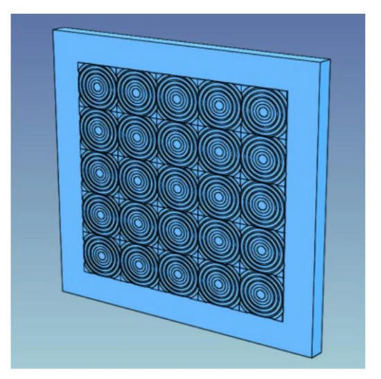
Diffractive microlenses are optical devices that use the Fourier optical principle to regulate the incident light. The diffractive microlens array produced by Coligh is a microarray structure manufactured using the diffractive optical principle. It consists of multiple diffractive microlenses arranged in a two-dimensional square matrix. It can correct high-order phase differences, achromatic aberrations, and achieve arbitrary wavefront modulation through surface relief structures, and realize the functions of controlling the phase of the incident light, focusing, splitting, multi-focus generation, and wavefront shaping of the light beam. Its application range is imaging and beam transformation, optical communication, medical cosmetology, and modulation of arbitrary spot distribution.
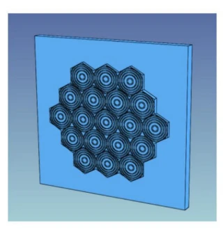
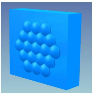
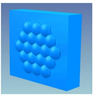
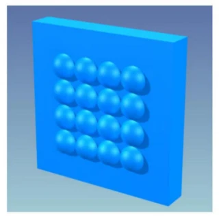
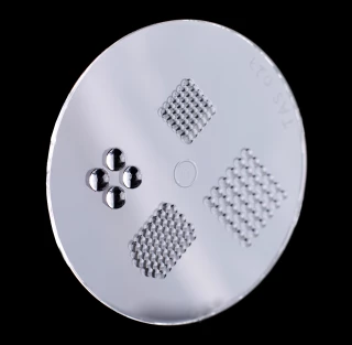
Microlens Shape: Square
Lens Arrangement: Square Grid
Lens Type: Refractive, Plano-Convex
Pitch Accuracy: ± 1 μm
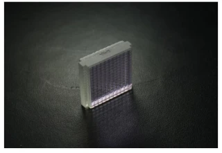
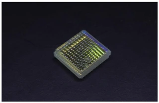
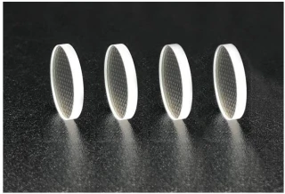
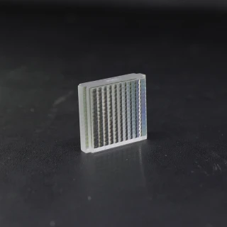
Square Diffractive Microlens Arrays
Specifications
| Material: | Fused Silica |
|---|---|
| Grid Shape: | Square |
| Effective Focal Length (EFL): | 10 mm |
| Lens Pitch: | 0.31 mm |
| Array Width: | 10 mm |
| Array Height: | 10 mm |
| Array Thickness: | 1 mm |
Got questions about specs? Use the inquiry form to ask.
Features
- We use 8-order phase design to improve the accuracy of wavefront control.
- The central wavelength covers from visible 550nm to mid-infrared 2940nm, which can adapt to different application requirements
- The sub-lens is square in shape, with sizes ranging from 310um to 1500um, which can adapt to beam shaping and collimation for different applications.
- We can provide two material options: fused quartz and single crystal silicon. Single crystal silicon is suitable for short-wave infrared and mid-infrared, and fused quartz is suitable for ultraviolet to near infrared.
- The microlens array can choose the thinnest thickness. The current standard product thickness is between 1mm-2mm. Single crystal silicon and fused use have excellent mechanical strength, thermal stability is also very good, and can adapt to the environment well.
Applications
- Fiber coupling: In fiber coupling, the beam quality, alignment accuracy and coupling efficiency are very high. If the laser energy is unevenly distributed, it will lead to low and unstable coupling efficiency. The square diffraction microlens array can achieve beam homogenization, collimation and beam splitting, allowing more light to enter the optical fiber
- Calibration: Lasers, sensors and imaging systems need to be optically calibrated during use. The square diffraction microlens array can divide a single laser beam into multiple highly uniform light spots, which can be used as a reference for calibration
- Imaging: In 3D cameras, infrared thermal imaging, medical imaging and other scenarios, it is necessary to control the uniformity of light and focus. The square diffraction microlens array can perform light homogenization and wavefront shaping in these imaging systems to improve the operating efficiency of the detector.
Similar Products
Need pricing for this product? Send a quick inquiry
Your inquiry has been received.
Create an account by adding a password
Why create an account?
- Auto-complete inquiry forms
- View and manage all your past messages
- Save products to your favorites
- Close your account anytime — no hassle