Description
Coligh manufactures and offer standard and custom Refractive Micro Lens Array, Diffractive Microlens Arrays, Linear Microlens Arrays, Cylindrical Microlens Arrays, Precision Diffraction Gratings, Diffractive Beam Splitters, Phase Optical Elements, Homogenizing Reflector,Test & Calibration Targets. Contact us for more information.
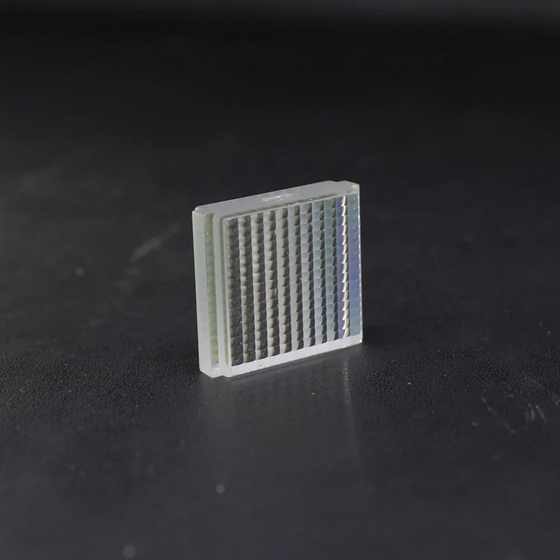
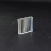
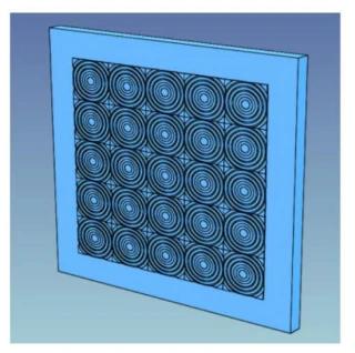
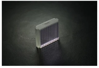
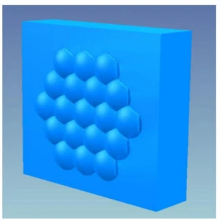
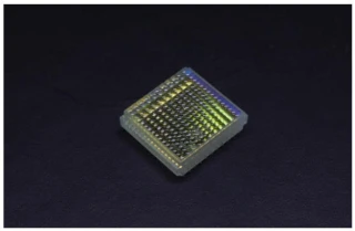
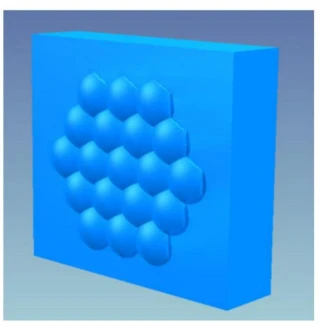
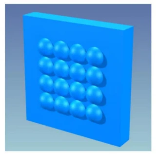
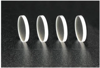
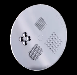
Lithography Microlens Arrays
Coligh Optics Technology Co.,ltd
Specifications
| Material: | IR Fused Silica, UV Fused Silica, Fused Silica |
|---|---|
| Grid Shape: | Square |
| Lens Pitch: | 0.01 mm |
| Array Width: | 10 mm |
| Array Height: | 10 mm |
| Array Thickness: | 1 mm |
| Pitch: | 10.0μm |
| EFFL: | 0.02 |
| ROC: | -0.0092 |
| Wavelength: | 0.6382 |
| Arrangement: | Square |
| Material: | Fused silica and Silicon |
Got questions about specs? Use the inquiry form to ask.
Features
- High-Precision Microlens Arrays: Designed to overcome challenges in traditional optical processing, such as high-order aspherical and freeform surfaces, small curvature radii, and small apertures.
- Advanced Fabrication: Capable of fabricating multiple lenses on a single glass substrate, offering enhanced efficiency and integration.
- Refractive Microlens Technology: Utilizes traditional geometric optics to provide smaller size, lighter weight, and higher integration compared to conventional optics.
- Versatile Applications: Ideal for imaging and beam shaping, CCD detection, optical communication, multi-beam scanning, CD/DVD read/write heads, and medical and beauty devices.
- Variety of Specifications: Available in different pitches, effective focal lengths, dimensions, and thicknesses to suit diverse application needs.
- Material and Design: Square aperture and square array design made from fused silica for durability and precision.
- Wide Range of Wavelengths: Supports various wavelengths, including 0.6328μm and 1.545μm, to accommodate different optical requirements.
- Comprehensive Product Range: Includes a variety of models with specific parameters for tailored performance in different optical systems.
Applications
- Beam shaping and homogenization: Used in laser systems to create uniform illumination profiles.
- Image enhancement: Improves light collection efficiency and resolution in CCD and CMOS sensors.
- Light field imaging: Enables 3D image capture and refocusing in light field cameras (e.g., Lytro).
- 3D displays / autostereoscopic displays: Enables glasses-free 3D by directing different views to each eye.
- Spectroscopy: Improves light collection in spectrometers and hyperspectral imaging systems.
- Confocal microscopy: Focuses excitation or collection light into multiple points for faster scanning.
- Wavefront sensing: Arrays of microlenses focus light from different parts of a telescope’s aperture to analyze distortions.
- Adaptive optics: Paired with deformable mirrors to correct atmospheric distortion in telescopes.
- Wafer inspection systems: Ensures uniform illumination and high-resolution scanning in semiconductor manufacturing.
- Optical profilometry: Used to focus and analyze surface topography.
- VCSEL coupling: Aligns vertical-cavity surface-emitting lasers with fiber arrays.
- Free-space optical interconnects: Facilitates efficient light coupling and multiplexing.
- Lab-on-chip and bio-sensors: Directs and focuses excitation light or collected signals in miniaturized detection systems.
Frequently Asked Questions
What are lithography microlens arrays?
Lithography microlens arrays are optical components made up of many tiny lenses arranged in a regular grid. They are fabricated using photolithographic techniques, allowing high precision and uniformity in lens shape, size, and placement.
Why are lithography microlens arrays preferred over molded arrays in some applications?
Lithography-based MLAs offer superior surface quality, tight dimensional tolerances, and better alignment precision. They are ideal for high-performance optics where uniformity and reproducibility are critical.
How are lithography microlens arrays used in laser beam shaping?
They homogenize or shape laser beams by splitting and overlapping light through individual lenslets, resulting in a uniform illumination profile at the output — essential for applications like laser projection and material processing.
What role do microlens arrays play in 3D displays?
In autostereoscopic 3D displays, MLAs direct different images to each eye without the need for glasses, enabling a glasses-free 3D viewing experience.
Can lithography MLAs improve sensor performance?
Yes. They focus incoming light onto the active area of image sensors (like CMOS or CCD), increasing light collection efficiency, reducing cross-talk, and improving image sharpness.
What materials are commonly used for lithography microlens arrays?
Typical materials include fused silica, polymers (e.g., SU-8), or glass substrates. The choice depends on wavelength requirements, thermal stability, and application.
Are lithography MLAs suitable for UV or IR applications?
Yes. With the right materials and design, lithographic MLAs can operate in UV, visible, or IR ranges. Fused silica MLAs, for instance, perform well in both UV and IR.
Got more questions? Use the RFQ form to ask the supplier directly.
Similar Products
Cylindrical Microlens Array
Coligh Optics Technology Co.,ltd
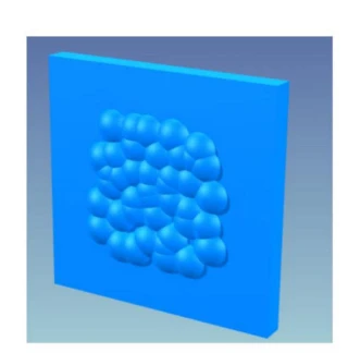
Random Aperture and Pattern Refractive Microlens Array
Coligh Optics Technology Co.,ltd
1D Circular Linear Microlens Array
Coligh Optics Technology Co.,ltd
Square Diffractive Microlens Arrays
Coligh Optics Technology Co.,ltd
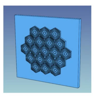
Hexagonal Diffractive Microlens Arrays
Coligh Optics Technology Co.,ltd
Silicon Square Microlens Array
Coligh Optics Technology Co.,ltd
Silicon Hexagonal Microlens Arrays
Coligh Optics Technology Co.,ltd
Fused Silica Square Microlens Arrays
Coligh Optics Technology Co.,ltd
Fused Silica Hexagonal Microlens Arrays
Coligh Optics Technology Co.,ltd
Circular Microlens Array with Square Grid
Coligh Optics Technology Co.,ltd
PicoLens High-Precision Microlens Array for Laser Medical Devices
CRYSTECH Inc.
Spherical Polymer Microlens Array
ORAFOL Fresnel Optics
Need pricing for this product? Send a quick inquiry
Thank You!
Your inquiry has been received.
Create an account by adding a password
Why create an account?
- Auto-complete inquiry forms
- View and manage all your past messages
- Save products to your favorites
- Close your account anytime — no hassle