
Optical Materials for Precision Light Transport
Frequently Asked Questions
What are optical materials and how are they used in photonic systems?
Optical materials are solids—typically glasses, crystals, polymers, or semiconductors—engineered for controlled interaction with electromagnetic radiation from UV to IR. They are used to fabricate lenses, prisms, windows, fibers, substrates, and nonlinear or active components, where properties like refractive index, transmission spectrum, and damage threshold directly determine system performance.
What key optical properties define material performance (e.g., refractive index, dispersion, transmission)?
Core parameters include refractive index n(λ), dispersion usually described by Abbe number or Sellmeier coefficients, and spectral transmission including absorption edges and bandgaps. Additional critical properties are scattering loss, birefringence, thermo-optic coefficient (dn/dT), and in some cases nonlinear coefficients (χ(2), χ(3)) or laser gain cross-sections for active media.
What are the main types of optical materials (glass, crystals, polymers, semiconductors) and how do they differ?
Optical glasses (e.g., BK7, fused silica) offer isotropic behavior, good manufacturability, and broad transparency, while crystalline materials (e.g., CaF2, sapphire, LiNbO3, YAG) can provide birefringence, nonlinear response, or laser gain. Polymers enable lightweight, moldable optics with moderate index control but typically lower thermal and environmental stability, and semiconductors (e.g., GaAs, InP, Si) are used for IR optics, detectors, and active photonic devices due to their direct or indirect bandgaps and high refractive indices.
Which parameters are most important when selecting an optical material for a given wavelength range?
You should first match the material’s transmission window and absorption edge to the operating wavelength, then evaluate refractive index, dispersion, and scattering losses at that wavelength. For high-power or pulsed systems, bulk and surface laser-damage thresholds, thermal conductivity, and dn/dT become equally critical to avoid thermal lensing and catastrophic damage.
How do mechanical, thermal, and environmental properties influence optical material choice?
Mechanical hardness, fracture toughness, and Young’s modulus govern how easily a material can be polished, its resistance to scratching, and its robustness in mounts. Thermal expansion coefficient, thermal conductivity, and operating temperature range determine dimensional and refractive stability, while chemical durability and moisture sensitivity (e.g., with hygroscopic crystals like KDP) dictate handling, packaging, and coating requirements.
What typical lead times, customization options, and cost drivers apply to optical materials?
Standard windows, substrates, and rods from common materials (e.g., fused silica, BK7) are often available from stock, whereas custom melts, dopant concentrations, crystal orientations, or large apertures can push lead times to 6–16 weeks. Cost is driven by raw material purity, boule or ingot growth complexity, size and yield, required homogeneity and surface quality, and secondary processing such as precision polishing, wedge control, or AR/HR coatings.
Engineered Optical Materials for Controlled Light Transport
Optical Materials are engineered solids used to guide, shape, transmit, or condition light in imaging, sensing, and laser systems. On FindLight you can source optical materials such as optical glass blanks and raw wafers that serve as the starting point for lenses, windows, filters, waveguides, and optoelectronic devices.
Optical Glass
Optical glass is a refined glass formulation with tightly controlled refractive index, Abbe number (dispersion), and homogeneity. These optical materials are typically supplied as blanks, rods, plates, or custom preforms that will be further ground, polished, and coated. Key parameters include refractive index tolerance, stress birefringence, internal transmittance over the target wavelength range (UV, visible, NIR, or SWIR), and coefficient of thermal expansion for athermal designs. Buyers should also verify bubble/striae class, surface quality if pre-polished, and compatibility with common AR or dielectric coatings.
Raw Wafers
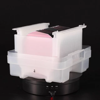
Raw wafers are crystalline or polycrystalline optical materials sliced and lapped to defined diameters and thicknesses for use in optoelectronics, photonics, and MEMS. Typical compositions include fused silica, sapphire, silicon, GaAs, and other III–V or II–VI semiconductors, selected according to the operational wavelength and required optical or electro‑optic behavior. Critical specifications include crystal orientation, doping type and level, resistivity, thickness tolerance, total thickness variation (TTV), bow/warp, surfaces (single‑ or double‑side polished), and surface roughness when low-scatter operation is required.
Buyer Guidance on FindLight
- Compare optical materials by wavelength transmission window, refractive index, dispersion, and thermal properties to match system design parameters.
- For optical glass, check catalog glass code, index/Abbe data, homogeneity class, and transmittance curves to ensure interchangeability with existing designs.
- For raw wafers, review datasheets for crystal orientation, defect density, flatness, and polishing grade to meet downstream processing requirements.
- Use FindLight to request quotes directly from suppliers of optical materials, attach drawings or specifications, and clarify tolerances or custom compositions. No registration is required to submit RFQs or contact vendors.
By evaluating these parameters, procurement engineers and researchers can identify optical materials that integrate cleanly into optical, photonic, and laser assemblies while controlling performance, yield, and lifecycle cost.