

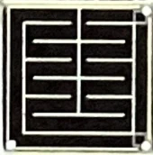
Description
The CCSiCUVPL265-A is a high-performance silicon carbide (SiC) ultraviolet linear photodiode designed for precise detection in the deep-UV to near-UV spectrum. Optimized for operation between approximately 200 nm and 375 nm, this device offers a highly selective response in the UV region, making it ideal for applications where visible light rejection and long-term stability are critical. Built on high-quality SiC epitaxial layers, the photodiode delivers reliable performance in demanding environments where conventional silicon-based detectors struggle or fail.
With a peak responsivity of about 0.137 A/W at 270 nm and a corresponding peak quantum efficiency of approximately 63%, the CCSiCUVPL265-A enables sensitive detection of low-level UV signals without the need for bulky optical filters. The device’s spectral response is tightly confined around the UV band, typically showing 90% of its maximum quantum efficiency in the 260–285 nm range and a full-width-at-half-maximum (FWHM) response from roughly 225–315 nm. This narrow, application-focused spectral window makes the photodiode particularly effective in systems that require precise discrimination of UV wavelengths while remaining effectively blind to visible light.
One of the defining advantages of this SiC photodiode is its exceptionally low dark current, typically below 500 fA per square millimeter at room temperature with a reverse bias under 3 V. This ultralow leakage current directly improves signal-to-noise ratio and minimizes the need for aggressive cooling strategies. Combined with a shunt resistance exceeding 250 GΩ/mm², the CCSiCUVPL265-A provides a stable, low-noise platform that is well suited for both high-sensitivity instrumentation and portable, power-conscious systems. Typical capacitance values, ranging from about 200 pF to 250 pF depending on active area, help support fast response times and straightforward integration into transimpedance amplifier or charge-sensitive readout circuits.
The inherent visible blindness of the SiC material system is a major benefit for UV-centric designs. In many UV sensors based on silicon, stray visible or near-infrared light must be blocked with additional optical filters and shielding. By contrast, the CCSiCUVPL265-A offers a visible-to-UV responsivity ratio greater than 5000 (comparing peak UV response to that at 400 nm), delivering a strong, selective UV signal with minimal interference from ambient lighting. This enables more compact optical assemblies, simplifies system design, and reduces overall cost by eliminating many external filtering components traditionally required in UV measurement setups.
The CCSiCUVPL265-A is engineered to operate over a very wide temperature range without significant performance degradation, a key advantage derived from its robust SiC construction. Devices of this class are known for tolerance to high junction temperatures, often up to several hundred degrees Celsius, and for excellent stability under continuous or pulsed UV irradiation. Such resilience makes the photodiode well suited for harsh industrial environments, outdoor installations, and systems exposed to strong UV flux, where detector longevity and calibration stability are essential. In many cases, the need for active thermal management can be reduced or eliminated, contributing to smaller system footprints and lower power consumption.
The active area options available within the CCSiCUVPL265-A family (for example, approximately 5.6 mm², 6.55 mm², and 7.06 mm² in the noted device variants) give designers flexibility in balancing sensitivity, capacitance, and layout constraints. A larger active area improves light collection and overall photocurrent, enhancing detectivity in low-flux scenarios, while moderate capacitance and carefully controlled series resistance (around 140–150 Ω, depending on variant) support stable, predictable behavior in a wide range of readout circuits. The device is commonly integrated using a simple transimpedance or integrating amplifier configuration, as illustrated in typical reference circuits, allowing straightforward coupling to both analog and digital processing chains.
The CCSiCUVPL265-A is particularly suitable for ultraviolet signal detection tasks where both accuracy and robustness are mandatory. Typical uses include water and air filtration monitoring, where the photodiode can be used to verify the intensity of germicidal UV-C lamps; pathogen detection and bio-analysis systems that rely on specific UV excitation bands; flame detection and combustion monitoring, where the sensor must reliably detect UV emissions in the presence of intense visible background.
CoolCAD CCSiCUVPL265 A SiC Ultraviolet Linear Photodiode 200 - 375nm
Specifications
| Diode Type: | Silicon Carbide (SiC) |
|---|---|
| Wavelength Of Operation (Typical): | 270 nm |
| Spectral Range: | 200 – 375 nm |
| Peak Responsivity (Rmax): | 0.137 A/W |
| Peak Quantum Efficiency: | 0.63 |
| Max Frequency Response: | Other / Not specified |
| Active Area: | 6.55 mm^2 |
| Package Type: | Bare Die |
| Built-In Amplifier: | No |
| Active Area (CCSiCUVPL265-A-27): | 6.55 mm² |
| Maximum Operating Temperature (no Degradation): | up to 400 °C |
| Shunt Resistance: | > 250 GΩ/mm² @ TA = 25 °C |
| Series Resistance (CCSiCUVPL265-A-25): | 150 Ω @ TA = 25 °C |
| Series Resistance (CCSiCUVPL265-A-27): | 140 Ω @ TA = 25 °C |
| Series Resistance (CCSiCUVPL265-A-28): | 150 Ω @ TA = 25 °C |
| Capacitance (CCSiCUVPL265-A-25): | 200 pF @ VR = 10 V, TA = 25 °C |
| Capacitance (CCSiCUVPL265-A-27): | 230 pF @ VR = 10 V, TA = 25 °C |
| Capacitance (CCSiCUVPL265-A-28): | 250 pF @ VR = 10 V, TA = 25 °C |
| Active Area (CCSiCUVPL265-A-25): | 5.6 mm² |
| Product: | SiC Ultraviolet Linear Photodiode |
| Active Area (CCSiCUVPL265-A-28): | 7.06 mm² |
| Visible Blindness Ratio: | > 5000 (peak responsivity / responsivity @ 400 nm, VR = 2 V) |
| Dark Current Density: | < 500 fA/mm² @ VR < 3 V, TA = 25 °C |
| Spectral Range (FWHM QE): | 225–315 nm @ VR < 3 V, TA = 25 °C |
| Spectral Range (90% Max QE): | 260–285 nm @ VR < 3 V, TA = 25 °C |
| Peak Quantum Efficiency: | 0.63 @ 270 nm, VR < 3 V, TA = 25 °C |
| Peak Responsivity: | 0.137 A/W @ 270 nm, VR < 3 V, TA = 25 °C |
| Part Number: | CCSiCUVPL265-A |
Got questions about specs? Use the inquiry form to ask.
 Download Data Sheet

Features
- Deep-UV Optimized SiC Photodiode (200–375 nm) – Specifically engineered silicon carbide (SiC) structure for reliable detection in the deep-ultraviolet region, ideal for applications around 265–270 nm.
- Narrowband UV Response with High Selectivity – Peak responsivity at 270 nm with spectral range (FWHM QE) from 225–315 nm and 90% peak QE between 260–285 nm, enabling highly selective UV detection with minimal out-of-band sensitivity.
- True Visible-Blind Operation – Inherent visible light blindness with a responsivity ratio > 5000 between peak UV and 400 nm, eliminating the need for external optical filters and improving signal-to-noise ratio in mixed light environments.
- Ultra-Low Dark Current for High Signal-to-Noise – Extremely low dark current < 500 fA/mm² (VR < 3 V, TA = 25°C) significantly reduces background noise, enabling precise low-level UV detection and accurate measurements.
- High Quantum Efficiency in the UV – Peak quantum efficiency of approximately 63% at 270 nm provides strong photocurrent output and higher sensitivity compared to many conventional Si-based UV photodiodes.
- High-Temperature Operation up to 400°C – Robust SiC material system and device design support operation over a wide temperature range with no degradation up to 400°C, reducing or eliminating active cooling requirements.
- Radiation-Hard and UV-Robust – Excellent resistance to long-term UV exposure and radiation damage ensures stable performance, long lifetime, and low drift in demanding industrial, aerospace, and scientific environments.
- Reduced System Complexity and Cost – Inherent visible-blindness, ultra-low dark current, and high-temperature tolerance allow removal of cooling assemblies and external filters, cutting system volume, power consumption, and overall cost of ownership.
- Multiple Active Area Options – Available as bare die variants (e.g., CCSiCUVPL265-A-28, -27, -25) with active areas typically around 5.6–7.06 mm², enabling optimization of responsivity, capacitance, and dynamic range for different optical setups.
- Low Capacitance for Fast Response – Device capacitance in the range of ~200–250 pF (VR = 10 V, TA = 25°C) supports high-speed readout and fast transient detection when paired with appropriate front-end electronics.
- High Shunt Resistance for Low Leakage – Shunt resistance > 250 GΩ/mm² enhances linearity at low light levels and minimizes leakage currents, ideal for precision metrology and low-light UV measurements.
- Stable Series Resistance for Consistent Performance – Series resistance on the order of 140–150 Ω provides predictable behavior under typical bias conditions and facilitates accurate modeling in circuit design.
- Bare Die Format for Custom Integration – Supplied as a bare die (marking: CCSiCUVPL265-A), allowing direct integration into custom packages, hybrid modules, or multi-channel linear arrays for compact OEM solutions.
- Compatible with Transimpedance and Integrating Readout Circuits – Designed for easy interfacing with standard photodiode readout topologies (TIA, integrating amplifiers), as demonstrated in typical reference circuits for low-noise UV detection.
- Ideal for Critical UV Sensing Applications – Optimized for ultraviolet signal detection in water monitoring, UV-based water filtration control, pathogen detection, flame detection, corona discharge sensing, UV curing control, and semiconductor/optical defect monitoring.
- High Reliability for Harsh Environments – SiC technology offers superior chemical and thermal stability, making these photodiodes suitable for outdoor, high-radiation, high-humidity, and chemically aggressive environments.
- Customizable Device Parameters – Fabricated on high-quality SiC epitaxial layers using proprietary processes, the devices can be customized (active area, geometry, array configuration) to meet application-specific optical and electrical requirements.
- Consistent, Linear Response Under UV Illumination – Well-behaved I–V characteristics and linear photocurrent response under 270 nm illumination provide predictable performance across a wide dynamic range.
- Optimized for 265–270 nm Disinfection and Sensing – Peak around 270 nm aligns with UVC wavelengths widely used in water disinfection and pathogen inactivation, making the CCSiCUVPL265-A especially effective in UV sterilization monitoring systems.
Applications
- Deep-UV and UV-C germicidal monitoring – Real-time monitoring of 254–280 nm UV-C sources in disinfection chambers, air purifiers, and surface sterilization systems to ensure sufficient dose for pathogen inactivation.
- Water purification and filtration systems – Feedback and safety monitoring of UV treatment lamps in municipal water plants, point-of-entry and point-of-use UV systems, wastewater treatment, and industrial process water sterilization.
- Pathogen and biohazard detection – Integration into portable and benchtop instruments that rely on UV-induced fluorescence or absorption for detecting bacteria, viruses, and biological contaminants in healthcare, food safety, and environmental monitoring.
- Flame detection and combustion monitoring – UV flame sensors for industrial burners, gas turbines, boilers, and furnaces, as well as safety interlocks in power plants, refineries, and process heaters where visible-blind operation prevents false alarms from hot surfaces.
- Corona and electrical discharge detection – Monitoring UV emission from partial discharges, arcs, and corona in high-voltage switchgear, transformers, power lines, and insulation systems for predictive maintenance.
- Plasma process monitoring – In-situ UV diagnostics of plasma in semiconductor fabrication tools (etching, deposition), surface treatment systems, and sputtering chambers, where high-temperature and radiation-hard detectors are required.
- UV curing control – Intensity and dose control of UV-curing systems for inks, adhesives, coatings, and 3D printing resins operating in the 200–375 nm range, enabling closed-loop lamp/LED regulation.
- Photolithography and resist processing – UV exposure monitoring in semiconductor photolithography steppers, mask aligners, PCB manufacturing, and microfabrication tools operating with i-line and deep-UV sources.
- Defect inspection and materials characterization – Detection of UV-induced luminescence or absorption contrast for defect mapping in wafers, optical coatings, crystals, and polymers; used in quality control of UV optics and coatings.
- Environmental UV monitoring – Measurement of solar UV-B and UV-C in atmospheric research, ozone-layer studies, and ground-based monitoring stations, leveraging visible-blind response to avoid background interference.
- UV index and solar safety instrumentation – Integration into UV meters and dosimeters for occupational safety, outdoor equipment testing, and monitoring of UV exposure on materials and surfaces.
- High-temperature sensing environments – UV detection in harsh conditions up to ~400 °C, such as engine compartments, exhaust systems, combustion chambers, and industrial furnaces where silicon photodiodes would fail or require cooling.
- Space and radiation-hard detectors – UV sensing in satellites, space telescopes, rocket plume diagnostics, and high-radiation environments where SiC’s robustness to ionizing radiation and long-term UV exposure is critical.
- UV spectroscopy and analytical instruments – Use in compact spectrometers and monochromator-based systems in the 225–315 nm FWHM band for chemical analysis, gas detection, and process analytics.
- Laser power and pulse monitoring (UV lasers) – Monitoring of 266 nm and 248–355 nm laser sources for alignment, power stabilization, and safety interlocks in scientific, industrial, and medical laser systems.
- Optical alignment and beam diagnostics in UV systems – Use as reference detectors for alignment of UV laser beams, LEDs, and lamp-based optics where visible-light suppression is required.
- UV LED binning, characterization, and production testing – Inline measurement of UV LED output (especially 255–285 nm emitters) for binning by radiant flux, wavelength, and stability in manufacturing lines.
- Non-destructive testing (NDT) with UV fluorescence – Intensity monitoring in fluorescent penetrant and magnetic particle inspection systems that use UV-A/B illumination while rejecting ambient visible light.
- Forensic and security imaging support – UV source monitoring in systems used for document verification, trace evidence analysis, and detection of security markings that fluoresce under deep UV.
- Scientific research and laboratory instrumentation – General-purpose UV detection in physics, chemistry, and biology labs for experiments involving UV-induced reactions, photochemistry, and spectroscopy.
Frequently Asked Questions
What is the CCSiCUVPL265-A SiC ultraviolet photodiode and what makes it different from a silicon UV photodiode?
What is the spectral response and quantum efficiency range of the CCSiCUVPL265-A SiC UV photodiode?
What are the key electrical characteristics (dark current, capacitance, resistance) of the CCSiCUVPL265-A?
What package options and active areas are available for the CCSiCUVPL265-A photodiode?
What are the typical applications of the CCSiCUVPL265-A SiC UV photodiode?
How should I bias and read out the CCSiCUVPL265-A photodiode in a circuit?
What are the advantages of using a SiC UV photodiode like CCSiCUVPL265-A for solar-blind or visible-blind detection?
Got more questions? Use the inquiry form to ask the supplier directly.
Similar Products


Your inquiry has been received.
Create an account by adding a password
Why create an account?
- Auto-complete inquiry forms
- View and manage all your past messages
- Save products to your favorites
- Close your account anytime — no hassle