

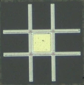
Description
The CCSiCUVPL02A is a high-performance silicon carbide (SiC) ultraviolet linear photodiode engineered for precise detection in the deep UV spectrum from approximately 200 nm to 375 nm. Built on high-quality SiC epitaxial layers, this bare die device offers a narrow spectral response centered around 290 nm, making it ideal for applications that demand true solar-blind operation, superior stability, and reliable UV measurement in demanding environments. Its visible-blind nature eliminates interference from ambient or artificial visible lighting, simplifying system design and improving signal integrity in UV-only sensing configurations.
In contrast to conventional silicon-based UV photodiodes, the CCSiCUVPL02A benefits from the intrinsic material properties of SiC, providing exceptionally low dark current and robust operation over a very wide temperature range, reportedly up to around 400 °C without performance degradation. The typical dark current is below 500 fA/mm² at room temperature, which significantly enhances signal-to-noise ratio, particularly in low-light or low-signal UV applications. With a peak responsivity of around 0.1 A/W and a peak quantum efficiency of approximately 43% at 290 nm, this device delivers dependable sensitivity to UV-C and neighboring UV-B wavelengths, while maintaining a very steep suppression of response in the visible region.
The CCSiCUVPL02A is designed to operate without the need for heavy thermal management or optical filtering, which can reduce overall system volume, cost, and complexity. Its inherent visible-blindness (with a visible rejection ratio exceeding 5000 at 400 nm) minimizes the need for additional optical filters that are typically required with silicon photodiodes for UV-selective measurements. At the same time, the proven resilience of SiC to long-term UV exposure and ionizing radiation enhances long-term stability, making this photodiode well-suited for continuous monitoring systems, harsh industrial environments, and outdoor or space-related deployments where lifetime and reliability are critical.
The spectral response of the CCSiCUVPL02A is tightly confined to the ultraviolet region. Around its peak, the 90% maximum quantum efficiency window lies roughly between 275 nm and 305 nm, and its full-width at half-maximum quantum efficiency extends from approximately 260 nm to 325 nm. This targeted response simplifies the design of UV-C and UV-B sensing systems, such as water and air purification monitoring, flame detection, pathogen detection, and defect inspection, where accurate differentiation between UV and visible components is essential. The active area of about 0.65 mm², combined with a typical capacitance of 50 pF at 10 V, supports both high sensitivity and fast response when paired with appropriate low-noise readout circuitry.
As a bare die component, the CCSiCUVPL02A offers flexibility for custom integration into specialized detector assemblies, multi-channel arrays, or compact sensor modules. Its typical series resistance of around 100 Ω and low parasitic capacitance make it compatible with transimpedance amplifier configurations and other standard photodiode readout topologies for precision photocurrent measurement. Integrators and system designers can take advantage of the proprietary SiC fabrication process behind this device to achieve tailored performance for specific spectral windows or operating conditions, enabling optimized UV sensing solutions for scientific, industrial, and safety-critical applications.
The combination of low noise, visible-blind UV selectivity, thermal robustness, and long-term UV stability places the CCSiCUVPL02A among the more advanced SiC photodiodes available in the market. It is a compelling choice for engineers who require accurate, reliable UV detection without the drawbacks associated with silicon-based detectors, especially where high ambient light, elevated temperature, or extended UV exposure would otherwise compromise conventional photodiodes. By leveraging these attributes, the CCSiCUVPL02A supports the design of compact, maintenance-friendly, and high-accuracy UV sensing systems across a broad range of emerging and established applications.
CCSiCUVPL02A SiC Ultraviolet Linear Photodiode 200 to 375 nm
Specifications
| Diode Type: | Silicon Carbide (SiC) |
|---|---|
| Wavelength Of Operation (Typical): | 285 nm |
| Spectral Range: | 200 – 375 nm |
| Peak Responsivity (Rmax): | 0.1 A/W |
| Peak Quantum Efficiency: | 0.43 |
| Max Frequency Response: | Other / Not specified |
| Active Area: | 0.65 mm^2 |
| Package Type: | Bare Die |
| Built-In Amplifier: | No |
| Part Number: | CCSiCUVPL02A |
| Peak Responsivity: | 0.1 A/W @ VR<3 V, λ=290 nm, TA=25°C |
| Peak Quantum Efficiency: | 0.43 @ VR<3 V, λ=290 nm, TA=25°C |
| Spectral Range (90% Max QE): | 275–305 nm @ VR<3 V, TA=25°C |
| Spectral Range (FWHM QE): | 260–325 nm @ VR<3 V, TA=25°C |
| Dark Current Density: | <500 fA/mm² @ VR<3 V, TA=25°C |
| Visible Blindness Ratio: | >5000 (peak responsivity / responsivity @ 400 nm, VR=2 V) |
| Post-exposure Responsivity Drift: | Negligible after 100 J/cm² @ 254 nm, VR=2 V |
| Capacitance: | 50 pF @ VR=10 V, TA=25°C |
| Series Resistance: | 100 Ω @ TA=25°C |
| Maximum Operating Temperature (no Degradation): | up to 400°C |
Got questions about specs? Use the inquiry form to ask.
 Download Data Sheet

Features
- Wide Ultraviolet Spectral Range (200–375 nm)
Optimized for UV-A and UV-C detection, providing reliable performance across a broad ultraviolet band for scientific, industrial, and safety applications. - High Peak Responsivity at 290 nm
Typical peak responsivity of 0.1 A/W at 290 nm and room temperature (VR < 3 V), enabling efficient conversion of UV radiation into measurable electrical signals. - Excellent Quantum Efficiency
Peak quantum efficiency of about 43% at 290 nm, delivering strong signal levels in demanding low-light or short-wavelength UV applications. - Narrowband UV Response for Improved Selectivity
90% maximum QE range from 275–305 nm and FWHM range from 260–325 nm, offering a well-defined and selective UV response that simplifies optical filtering and system design. - Inherently Visible-Blind Operation
Extremely low sensitivity to visible light, with a responsivity ratio > 5000:1 (peak responsivity vs. 400 nm), eliminating the need for additional visible-blocking filters and improving UV signal purity. - Ultra-Low Dark Current for High Signal-to-Noise
Typical dark current of < 500 fA/mm² at VR < 3 V and 25°C, minimizing noise and enabling precise detection of very low UV flux in laboratory and field environments. - Stable Performance Over Wide Temperature Range
Silicon carbide (SiC) design supports operation up to approximately 400°C with no significant degradation, ideal for harsh or high-temperature environments where silicon photodiodes fail. - Outstanding UV and Radiation Robustness
Minimal responsivity drift even after 100 J/cm² total exposure at 254 nm, ensuring long-term stability, low maintenance, and reliable calibration in high UV dose environments. - No Cooling or Optical Filters Required in Most Setups
Combination of low dark current, visible-blind response, and high-temperature capability reduces or eliminates the need for active cooling and external filtering, lowering system size, cost, and complexity. - Compact Active Area for Precision Measurements
Active area of approximately 0.65 mm², enabling focused beam measurements, array configurations, and integration into compact optical assemblies. - Low Capacitance for Fast Response
Typical junction capacitance of about 50 pF at VR = 10 V, supporting fast temporal response for pulsed UV sources, time-resolved measurements, and high-speed detection electronics. - Robust Series Resistance Characteristics
Typical series resistance of about 100 Ω, allowing straightforward matching to transimpedance amplifiers and low-noise readout electronics. - Linear Photodiode Operation
Designed as a linear SiC UV photodiode, providing a proportional output over a wide dynamic range for accurate quantitative UV measurements. - Bare-Die Format for Custom Integration
Supplied as bare die (Part Number CCSiCUVPL02A), giving designers flexibility to integrate directly into custom packages, optical heads, sensor arrays, or hybrid modules. - Customizable Through Proprietary SiC Processes
Fabricated on high-quality SiC epitaxial layers with proprietary processing, allowing customization of geometry, packaging, and performance parameters for OEM and specialized applications. - Ideal for Critical UV Monitoring Applications
Well-suited for ultraviolet signal detection, water filtration and purification systems, pathogen detection, flame and combustion monitoring, UV curing control, and defect/contamination monitoring in industrial lines. - High Reliability in Harsh Environments
SiC technology resists degradation from intense UV exposure, radiation, and extreme temperatures, providing long operating lifetimes in aerospace, automotive, sterilization, and outdoor installations. - Easy Integration with Standard Readout Circuits
Compatible with typical transimpedance amplifier configurations, enabling straightforward implementation in existing UV sensor platforms and measurement electronics. - ESD-Sensitive, High-Quality Semiconductor Construction
Manufactured to advanced semiconductor standards with attention to electrostatic discharge precautions, supporting consistent, repeatable performance across device batches.
Applications
The CCSiCUVPL02A is a visible-blind, low-dark-current SiC UV photodiode optimized for narrowband detection around 260–325 nm, with high quantum efficiency at 290 nm and robust performance up to elevated temperatures. These characteristics enable or simplify a wide range of industrial, scientific, medical, environmental, and safety applications where reliable UV-A/UV-B/UV-C detection is critical.
UV Disinfection and Sterilization- UV-C germicidal lamp monitoring in air, surface, and object disinfection systems
- Real-time dose control for UV-C LED and mercury-lamp sterilizers (hospitals, labs, public facilities)
- UV disinfection efficacy verification in HVAC systems, air purifiers, and upper-room UVGI installations
- Closed-loop feedback for maintaining target irradiance and compensating lamp aging
- UV water filtration and purification systems – residential, commercial, and municipal
- UV dose monitoring in drinking water and wastewater UV reactors
- Online sensor modules for UV reactor performance validation and regulatory compliance
- LED-based UV water sterilizers for point-of-use and portable systems
- Fluorescence and absorption-based pathogen detection using UV excitation in microbiology and diagnostics
- Biohazard and contamination monitoring in cleanrooms, pharmaceutical facilities, and food production
- Field-deployable biosensors for rapid detection of bacteria, viruses, and spores with UV-induced signatures
- UV flame detectors for gas turbines, boilers, burners, furnaces, and industrial heaters
- Explosion-proof flame sensors in refineries, petrochemical plants, and power stations
- High-speed flame monitoring in combustion research and burner characterization
- Fire and spark detection in dust explosions and high-risk processing lines
- Plasma process monitoring in PECVD, RIE, and other plasma etch/deposition tools via UV emission
- UV curing systems for inks, coatings, adhesives, and resins (dose control and uniformity mapping)
- Process endpoint detection using UV spectral signatures in semiconductor manufacturing
- High-temperature in-situ monitoring in harsh process environments where Si photodiodes degrade
- Defect inspection of wafers, PCBs, glass, and polymer films using UV contrast
- Surface contamination detection (organic residues, films, and particles) under UV illumination
- Coating thickness and uniformity verification via UV reflectance/transmission measurements
- Industrial quality control in printed electronics, packaging, and UV-sensitive marking
- Solar UV-A/UV-B monitoring for environmental stations and climatological studies
- UV index meters and dosimeters for personal and professional use
- Atmospheric and ozone layer research using 260–325 nm spectral response
- Outdoor UV monitoring of material exposure and weathering tests
- UV-based presence and position sensing where visible light interference must be rejected
- UV signature monitoring in chemical processes and reactors
- Verification of UV-activated inks and security features in packaging and labeling lines
- On-line monitoring of UV-emitting processes for predictive maintenance
- Non-destructive testing (NDT) using UV excitation and fluorescent penetrants
- Forensic analysis of bodily fluids, fibers, and residues under UV illumination
- Document and currency authentication via UV security features
- Anti-counterfeiting systems in brand protection and supply-chain security
- UV spectrophotometers and monochromators in the 200–375 nm band
- Fluorometers and UV-sensitive detectors for biochemical and analytical assays
Frequently Asked Questions
What is the CCSiCUVPL02A SiC ultraviolet photodiode and what wavelength range does it cover?
Why choose a SiC UV photodiode like CCSiCUVPL02A instead of a silicon UV photodiode?
What are the main applications of the CCSiCUVPL02A UV photodiode?
What are the key electrical and optical characteristics of the CCSiCUVPL02A photodiode?
Is the CCSiCUVPL02A UV photodiode truly visible-blind, and do I need an additional optical filter?
How do I bias and read out the CCSiCUVPL02A SiC UV photodiode in a circuit?
What package options, customization possibilities, and reliability considerations are there for the CCSiCUVPL02A?
Got more questions? Use the inquiry form to ask the supplier directly.
Similar Products


Your inquiry has been received.
Create an account by adding a password
Why create an account?
- Auto-complete inquiry forms
- View and manage all your past messages
- Save products to your favorites
- Close your account anytime — no hassle