

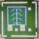
Description
The CCSiCUVPL01 series of silicon carbide (SiC) ultraviolet linear photodiodes is engineered for high‑precision UV detection in demanding industrial, scientific, and environmental monitoring applications. Designed to operate optimally in the 200–375 nm spectral region, these devices provide a tightly controlled response within the germicidal and solar‑blind UV bands, while remaining effectively insensitive to visible light. This inherent UV selectivity dramatically simplifies optical design by reducing or eliminating the need for external filters that are typically required with conventional silicon photodiodes.
Fabricated on high‑quality SiC epitaxial layers using advanced proprietary processes, the CCSiCUVPL01 delivers a combination of very low dark current, high quantum efficiency, and long‑term stability under intense UV exposure. With peak responsivity around 0.112 A/W at 265 nm and a peak quantum efficiency of approximately 54% at 245 nm, these photodiodes are optimized for accurate detection of low‑level UV signals. The typical spectral response is tightly confined, with a 90% maximum QE range of about 235–270 nm and a full‑width‑half‑maximum response spanning roughly 225–315 nm, making them ideal for applications that demand narrowband UV performance.
One of the defining advantages of this SiC photodiode line is its exceptionally low dark current, on the order of a few hundred femtoamps per square millimeter at modest reverse bias (VR < 3 V, TA = 25 °C). Such low noise performance enables high signal‑to‑noise ratios even in compact readout circuits and allows reliable measurements at very low UV intensities. The low junction capacitance (with typical values of 17–37 pF depending on active area) and well‑controlled series resistance further support fast response and clean signal readout in both linear and pulse‑sensing configurations.
In contrast to traditional silicon‑based UV detectors, the CCSiCUVPL01 is intrinsically “visible‑blind.” The ratio of its peak UV responsivity to the responsivity at 400 nm exceeds 5000, meaning that visible and near‑IR wavelengths contribute negligibly to the output signal. This property is particularly valuable in outdoor and industrial environments where strong ambient visible illumination can easily saturate or distort measurements from standard photodiodes. By rejecting visible light at the material level rather than via external optics, the device helps minimize stray‑light errors and simplifies system‑level optical and mechanical design.
The robust SiC material system also offers outstanding thermal and radiation stability. The CCSiCUVPL01 is built to maintain performance across a wide temperature range, with no fundamental material‑related degradation up to very high operating temperatures. The devices demonstrate negligible responsivity drift even after substantial cumulative UV exposure (e.g., 100 J/cm² at 254 nm under typical test conditions), making them well suited for long‑life installations. This reliability in harsh environments supports deployment in UV sterilization equipment, combustion monitoring, aerospace and spaceborne instruments, and industrial process control where both radiation hardness and thermal endurance are critical.
Multiple active‑area variants within the CCSiCUVPL01 family (approximately 0.24 mm², 0.38 mm², and 0.52 mm²) allow designers to trade off sensitivity, capacitance, and speed according to system requirements. Larger areas deliver higher photocurrent for a given irradiance, enhancing sensitivity and easing the design of low‑noise front‑end electronics, while smaller areas reduce capacitance for faster response and lower noise in high‑bandwidth applications. These devices are typically provided as bare die, enabling seamless integration onto custom PCBs, hybrid modules, or focal plane assemblies, and giving designers the freedom to define bespoke packaging and optical configurations.
Typical use cases include ultraviolet signal detection, water and air purification monitoring, and UV‑C source calibration, where accurate dosage measurements around 254–275 nm are essential for system safety and regulatory compliance. The devices are also well suited to pathogen detection systems, flame detection and combustion monitoring, early fire warning systems, and defect inspection in semiconductor, glass, and specialty materials manufacturing. In many of these applications, the combination of high UV sensitivity, low dark noise, and visible blindness enables more compact, lower‑power, and more reliable sensing modules than those based on silicon or photomultiplier technologies.
System integration is further simplified by the compatibility of the CCSiCUVPL01 with standard low‑voltage bias and conventional transimpedance amplifier topologies.
CoolCAD CCSiCUVPL01 SiC Ultraviolet Linear Photodiode 200-375nm Bare Die
Specifications
| Diode Type: | Silicon Carbide (SiC) |
|---|---|
| Wavelength Of Operation (Typical): | 245 nm |
| Spectral Range: | 200 – 375 nm |
| Peak Responsivity (Rmax): | 0.112 A/W |
| Peak Quantum Efficiency: | 0.54 |
| Max Frequency Response: | Other / Not specified |
| Active Area: | 0.38 mm^2 |
| Package Type: | Bare Die |
| Built-In Amplifier: | No |
| Part Number: | CCSiCUVPL01 |
| Peak Responsivity: | 0.112 A/W @ VR<3 V, λ=265 nm, TA=25 °C |
| Peak Quantum Efficiency: | 0.54 @ VR<3 V, λ=245 nm, TA=25 °C |
| Spectral Range 90% Max QE: | 235–270 nm @ VR<3 V, TA=25 °C |
| Spectral Range FWHM QE: | 225–315 nm @ VR<3 V, TA=25 °C |
| Dark Current: | <500 fA/mm² @ VR<3 V, TA=25 °C |
| Visible Blindness Ratio: | >5000 (peak responsivity / responsivity @ 400 nm, VR=2 V |
| Active Area CCSiCUVPL01A: | 0.52 mm² |
| Active Area CCSiCUVPL01B: | 0.38 mm² |
| Active Area CCSiCUVPL01C: | 0.24 mm² |
| Capacitance CCSiCUVPL01A: | 37 pF @ VR<3 V, TA=25 °C |
| Capacitance CCSiCUVPL01B: | 27 pF @ VR<3 V, TA=25 °C |
| Capacitance CCSiCUVPL01C: | 17 pF @ VR<3 V, TA=25 °C |
| Series Resistance CCSiCUVPL01A: | 200 Ω @ TA=25 °C |
| Series Resistance CCSiCUVPL01B: | 175 Ω @ TA=25 °C |
| Series Resistance CCSiCUVPL01C: | 230 Ω @ TA=25 °C |
| Operating Wavelength Range (application Description): | 200–375 nm |
| Maximum Operating Temperature (no Degradation): | up to 400 °C |
Got questions about specs? Use the inquiry form to ask.
 Download Data Sheet

Features
- Deep-UV Optimized SiC Photodiode (200–375 nm) – Engineered on high‑quality silicon carbide epitaxial layers for reliable, linear detection in the ultraviolet range, ideal for applications requiring precise UV-A and UV-C sensitivity.
- Visible-Blind for High Signal-to-Noise in UV – Inherent visible light blindness (UV-only response) with visible blindness ratio > 5000 (peak responsivity / responsivity at 400 nm) minimizes interference from ambient light and eliminates the need for optical visible-blocking filters.
- Exceptionally Low Dark Current – Typical dark current < 500 fA/mm² at VR < 3 V and TA = 25 °C, comparable to or better than leading SiC and GaN UV photodiodes, enabling detection of very low UV light levels with excellent noise performance.
- High Quantum Efficiency in UV – Peak quantum efficiency of approximately 54% (η ≈ 0.54) at 245 nm and peak responsivity of about 0.112 A/W at 265 nm (VR < 3 V, TA = 25 °C), delivering strong electrical output per incident UV photon.
- Narrow, Well-Defined UV Spectral Response – 90% maximum QE range of 235–270 nm and FWHM QE range of 225–315 nm provide a tight spectral window for targeted UV detection without broadband background, suited for analytical and monitoring systems.
- Wide Temperature Range Operation up to 400 °C – Robust SiC material system enables operation over an extremely wide temperature range with no degradation reported up to 400 °C, supporting deployment in harsh industrial, aerospace, and engine environments.
- Excellent UV and Radiation Robustness – Long‑term UV exposure stability with negligible responsivity drift after 100 J/cm² at 254 nm (VR = 2 V), plus strong resistance to radiation damage, reduces recalibration frequency and extends system lifetime versus silicon UV photodiodes.
- Reduced Cooling Requirements and System Volume – Low dark current, high-temperature tolerance, and visible blindness significantly reduce or eliminate the need for active cooling, optical filters, and complex shielding, enabling more compact and energy‑efficient UV detection modules.
- Multiple Active Area Options – Available in several active area sizes (e.g., CCSiCUVPL01A ≈ 0.52 mm², CCSiCUVPL01B ≈ 0.38 mm², CCSiCUVPL01C ≈ 0.24 mm²) to optimize between sensitivity, speed, and capacitance for different system designs.
- Low Capacitance for Fast Response – Typical capacitances of about 37 pF (A), 27 pF (B), and 17 pF (C) at VR < 3 V support faster response times and higher bandwidth operation, suitable for pulsed UV sources and high‑speed monitoring.
- Moderate Series Resistance for Efficient Readout – Series resistance in the 175–230 Ω range (depending on active area) is compatible with standard transimpedance amplifier (TIA) circuits and low‑noise readout architectures used in precision UV detection.
- Bare Die Format for Flexible Integration – Supplied as a bare die (CCSiCUVPL01) to allow custom packaging, hybrid integration, or direct attachment onto PCBs, ceramic substrates, or optical benches for maximum layout flexibility.
- Customizable Design and Fabrication – Proprietary SiC fabrication processes enable customization of active area, geometry, and packaging to match specific OEM specifications, wavelength bands, and system‑level performance targets.
- Linear Photodiode Response – Designed as a linear UV photodiode for proportional response to incident UV intensity, simplifying calibration and enabling accurate quantitative measurements in sensing and metrology applications.
- Compatible with Standard UV Readout Circuits – Works seamlessly with classic transimpedance amplifier configurations (integrator/TIA) for both DC and pulsed UV measurements, easing integration into existing electronic platforms.
- Ideal for Critical UV Applications – Optimized for UV signal detection in:
- Water and air purification / filtration systems (UV-C monitoring)
- Pathogen and contamination detection
- Flame detection and combustion monitoring
- Defect and surface inspection in semiconductor and industrial processes
- Environmental UV index and UV process control
- High Reliability for Demanding Environments – SiC device physics and rugged construction provide high reliability under high temperature, high UV flux, and radiation‑rich conditions where conventional silicon photodiodes rapidly degrade.
Applications
- Ultraviolet flame detection and monitoring in industrial burners, gas turbines, oil and gas boilers, and combustion systems, where visible-blind UV response prevents false triggers from hot surfaces and ambient light.
- Fire and spark detection in critical infrastructure, power plants, aircraft engines, and transportation tunnels, leveraging fast UV response for early-stage fire and arc detection.
- Gas and chemical flame monitoring in hazardous environments (refineries, chemical plants, paint booths) where reliable UV flame presence detection is required under intense visible/IR backgrounds.
- Ultraviolet water disinfection monitoring in UV-C water purification systems for municipal, industrial, and residential water treatment, to verify lamp output and dosage in the 200–280 nm germicidal range.
- UV reactor dose measurement in advanced oxidation and wastewater treatment plants, ensuring accurate UV intensity feedback for process control and regulatory compliance.
- Pathogen and bio-agent detection using UV fluorescence or direct UV absorption for bacteria, viruses, spores, and biological contaminants in medical, environmental, and food-safety applications.
- Air and surface sterilization system monitoring in HVAC UVGI systems, hospital and laboratory sterilizers, and cleanroom equipment to confirm germicidal lamp performance over time.
- UV curing process control for inks, coatings, adhesives, and resins, providing closed-loop feedback in industrial curing lines operating in the UV-C/UV-B range.
- Semiconductor wafer and mask inspection where short-wavelength UV is used to reveal submicron defects, pattern non-uniformities, or contamination that are not visible with longer wavelengths.
- Photolithography process monitoring in semiconductor and MEMS fabrication, including alignment, exposure dose verification, and UV tool health monitoring.
- LCD, OLED, and microdisplay inspection using UV illumination to detect pixel defects, contamination, and coating non-uniformities while remaining blind to ambient room lighting.
- Solar-blind UV imaging and detection in the 200–280 nm band, eliminating interference from sunlight and visible light for outdoor sensing applications.
- Corona discharge and partial discharge detection on high-voltage transmission lines, switchgear, and insulators, where UV emissions indicate insulation breakdown and early failure.
- Electric arc and plasma monitoring in welding, plasma cutting, sputtering, and other high-energy processes, using UV signatures to control process parameters and ensure operator safety.
- Combustion diagnostics in research engines, gas turbines, and industrial furnaces, using UV emission and absorption to study flame fronts, fuel-air mixing, and pollutant formation.
- UV spectroscopy and analytical instrumentation for absorbance and fluorescence measurements in the deep-UV range (e.g., 220–300 nm) in chemistry, life sciences, and environmental labs.
- Protein, nucleic acid, and aromatic compound detection at UV absorbance peaks (e.g., ~260–280 nm) in bioanalytical instruments, lab-on-chip devices, and microfluidic systems.
- Environmental UV monitoring of artificial UV-C and UV-B sources in laboratories, sterilization chambers, and industrial plants, where visible-blindness simplifies measurements.
- UV index and radiation safety monitoring around high-intensity UV-C sources in research labs, semiconductor fabs, and disinfection systems to protect personnel.
- Non-destructive testing (NDT) with UV using fluorescent penetrants and magnetic particles, where deep-UV excitation improves contrast and defect visibility.
- Materials and coating degradation studies under accelerated UV exposure, mapping reflectivity, transmittance, yellowing, and microcracking of polymers, paints, and encapsulants.
- Quality control of UV-transparent optics such as fused silica, sapphire, and UV-grade lenses, by measuring transmission and scattering in the 200–300 nm range.
- High-temperature UV sensing in furnaces, engines, and exhaust systems, taking advantage of SiC’s stability up to very high temperatures where silicon photodiodes fail.
- Harsh-environment monitoring in aerospace, automotive, and downhole applications where wide temperature range and radiation hardness are required.
Frequently Asked Questions
What is the CCSiCUVPL01 SiC ultraviolet photodiode and what wavelength range does it cover?
How is this SiC UV photodiode different from a standard silicon UV photodiode?
What are typical performance characteristics such as responsivity, quantum efficiency, and dark current?
What active area options and electrical parameters are available for the CCSiCUVPL01?
What are the main applications of the CCSiCUVPL01 SiC UV photodiode?
How should the CCSiCUVPL01 SiC UV photodiode be biased and connected in a readout circuit?
Can the CCSiCUVPL01 be customized or integrated into specific UV detection systems?
Got more questions? Use the inquiry form to ask the supplier directly.
Similar Products


Your inquiry has been received.
Create an account by adding a password
Why create an account?
- Auto-complete inquiry forms
- View and manage all your past messages
- Save products to your favorites
- Close your account anytime — no hassle