

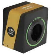
Description
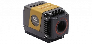
The SID4 XHR is a cutting-edge wavefront sensor designed to deliver exceptional performance in a remarkably compact form factor. Engineered for applications demanding extreme high resolution, this device stands out with its large sensor area and advanced phase measurement capabilities. Its wavelength range of 400 to 1100 nm makes it highly versatile, accommodating a broad spectrum of optical testing and metrology tasks in research, industrial, and quality control environments.
At the heart of the SID4 XHR is a generously sized aperture measuring 38.64 x 27.60 mm², enabling the analysis of large optical beams without compromising on detail. The sensor boasts a phase sampling grid of 1400 x 1000, resulting in a fine spatial resolution of 27.6 µm. This allows for the precise characterization of complex wavefronts, making it ideal for demanding applications such as laser beam diagnostics, optical component testing, and adaptive optics.
The device achieves an impressive phase resolution of 6 nm RMS, ensuring accurate and repeatable measurements even for subtle wavefront aberrations. Despite its advanced capabilities, the SID4 XHR maintains a compact footprint with dimensions of 114 x 105 x 110 mm and a lightweight design at approximately 1 kg. This makes it easy to integrate into existing setups or deploy in space-constrained environments.
With its plug-and-play operation, the SID4 XHR streamlines the measurement process, reducing setup time and facilitating rapid data acquisition. Its robust construction and user-friendly interface cater to both laboratory and industrial users seeking reliable, high-precision wavefront analysis. The SID4 XHR sets a new standard for high-resolution, compact wavefront sensing, empowering users to push the boundaries of optical measurement and control.
SID4 XHR High Resolution Phase Sensor 400-1100nm Compact Plug and Play
Specifications
| Wavelength Range: | 400 – 1100 nm |
|---|---|
| # Pixels (Width): | 1400 |
| # Pixels (Height): | 1000 |
| Lenslet Pitch: | 27.6 um |
| Wavefront Accuracy: | Unspecified |
| Type: | Lateral Shearing |
| Aperture Dimension: | 38.64 x 27.60 mm² |
| Phase Sampling: | 1400 x 1000 |
| Spatial Resolution: | 27.6 µm |
| Phase Resolution: | 6 nm RMS |
| Dimensions: | 114 x 105 x 110 mm |
| Weight: | ~1 kg |
Got questions about specs? Use the inquiry form to ask.
 Download Data Sheet

Features
- Ultra-High Resolution Phase Imaging: Achieve exceptional phase sampling of 1400 x 1000 with a phase resolution of 6 nm RMS for precise optical measurements.
- Large Sensor Aperture: Features a generous 38.64 x 27.60 mm² aperture, enabling wide field-of-view and high sensitivity for diverse applications.
- Broad Wavelength Range: Operates efficiently across 400 – 1100 nm, covering visible to near-infrared spectral regions for versatile use.
- Compact & Lightweight Design: Space-saving dimensions (114 x 105 x 110 mm) and lightweight (~1 kg) construction make it ideal for integration into laboratory and industrial setups.
- High Spatial Resolution: Delivers a spatial resolution of 27.6 µm, ensuring detailed and accurate imaging of fine structures.
- Plug and Play Operation: User-friendly setup with minimal configuration required, allowing for quick deployment and ease of use.
- Robust & Reliable: Engineered for stability and consistent performance in demanding environments.
- Versatile Applications: Perfect for quantitative phase imaging, wavefront sensing, laser beam characterization, and optical metrology.
- Trusted Manufacturer: Developed by PHASICS, a global leader in advanced optical instrumentation.
Applications
- Laser Beam Characterization: Accurately measure and analyze laser beam profiles, wavefronts, and phase distortions for research, development, and quality control in optics and photonics.
- Optical Component Testing: Evaluate the quality and performance of lenses, mirrors, and other optical components by detecting aberrations and surface defects with high spatial and phase resolution.
- Microscopy and Bio-Imaging: Enhance quantitative phase imaging in biological and medical research, enabling label-free cell analysis, tissue imaging, and live cell monitoring.
- Semiconductor Inspection: Perform non-contact, high-resolution inspection of wafers and photomasks to detect sub-micron defects and ensure process quality in semiconductor manufacturing.
- Adaptive Optics: Integrate into adaptive optics systems for real-time correction of wavefront distortions in astronomy, laser communication, and ophthalmology.
- Metrology and Surface Profiling: Conduct precise surface topography measurements for industrial metrology, MEMS characterization, and quality assurance of precision surfaces.
- Laser System Alignment: Facilitate rapid and accurate alignment of complex laser systems and optical setups, reducing setup time and improving performance.
- Material Science Research: Investigate material properties, stress, and deformation by mapping phase variations across samples in materials research and engineering.
- Optical System Development: Support the design, testing, and optimization of advanced optical systems, including telescopes, microscopes, and imaging devices.
- Educational and Training Purposes: Serve as a powerful teaching tool for demonstrating principles of wavefront sensing, phase imaging, and optical metrology in academic settings.
Frequently Asked Questions
What is the SID4 XHR and what are its main applications?
What wavelength range does the SID4 XHR support?
What are the key specifications of the SID4 XHR wavefront sensor?
How does the SID4 XHR compare to other wavefront sensors?
Is the SID4 XHR easy to integrate and use?
What industries or research fields benefit most from the SID4 XHR?
Where can I get technical support or more information about the SID4 XHR?
Got more questions? Use the inquiry form to ask the supplier directly.
Similar Products

Your inquiry has been received.
Create an account by adding a password
Why create an account?
- Auto-complete inquiry forms
- View and manage all your past messages
- Save products to your favorites
- Close your account anytime — no hassle