
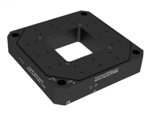
Description
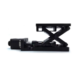
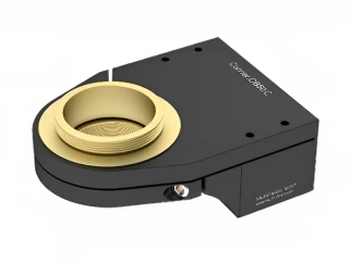
The Carrier.S100-OB.Z from MultiFields Technologies is a high-performance, compact piezoelectric Z-stage designed for objective autofocus scanning in demanding applications such as precision optics, semiconductor characterization, and research microscopy. Engineered for stability, accuracy, and ultra-fast response, this stage provides a 100 μm travel range along the Z-axis with sub-nanometer resolution.
Utilizing a high-quality resistive sensor and piezoelectric motion technology, the system achieves closed-loop positioning with less than 1 nm accuracy and a rapid 90% position stabilization in just 15 ms. Its durable stainless steel and aluminum alloy frame supports a maximum load of 500 g, ensuring structural rigidity and performance consistency.
Compatible with MultiFields® Archimedes Series motion controllers, the Carrier.S100-OB.Z also offers upgrade options for non-magnetic and ultra-high vacuum environments. Designed to meet the rigorous demands of next-generation scanning applications, this objective stage delivers precise, reliable, and fast motion—making it an essential tool in modern nano-positioning platforms.
Room Temperature Carrier.S100-OB. Z Objective Autofocus Scanning Table
Specifications
| Load Capacity: | 0.5 kg |
|---|---|
| Vacuum Compatible: | Yes |
| Microstep Size (default Resolution): | 0.0001 um |
| Built-in Controller: | No |
| Travel Range: | 0.1 mm |
| Accuracy (unidirectional): | 0.0003 um |
| Backlash: | ≤5 um |
| Loaded Backlash (10 N): | Not Specified |
| Maximum Speed: | Not Specified |
| Weight: | 0.27 kg |
| Guiding Mechanism: | Other |
| Voltage Requirement: | DC 24V |
| Pitch / Yaw: | 30 urad |
| Position Encoder: | Resistive Sensor |
| Sensor Noise: | 0.3 nm |
| Z-axis Resolution (Open-loop): | 0.1 nm |
| Stabilize Time (90% Position): | 15 ms |
| Rigidity: | 0.4 N/um |
| Resonant Frequency (No Load): | 650 Hz |
| Weight: | 270 g |
| Main Body: | Stainless Steel 304, Aluminum Alloy |
Got questions about specs? Use the inquiry form to ask.
Features
- 100 µm Z-Axis Travel Range: Enables high-precision vertical motion for objective scanning tasks
- Sub-Nanometer Closed-Loop Resolution: Delivers ultra-fine positioning with better than 1 nm accuracy using resistive feedback sensors
- Fast Stabilization: Achieves 90% position stability within just 15 milliseconds, ensuring rapid response in dynamic systems
- Compact & Rigid Design: High structural rigidity of 0.4 N/µm in a compact footprint supports stability and precision
- High Load Capacity: Capable of supporting up to 500 g for compatibility with a wide range of optical or mechanical payloads
- Ultra-Low Sensor Noise: Provides reliable feedback with only 0.3 nm of sensor noise
- Vacuum & Magnetic Compatibility: Available in non-magnetic (.NM) and ultra-high vacuum (.UHV) configurations for specialized environments
- Controller Integration: Seamlessly interfaces with MultiFields® Archimedes Series motion controllers for optimized system control
Applications
- Objective Autofocus Scanning: Ideal for high-resolution microscopy systems requiring accurate and fast Z adjustments
- Precision Optics Alignment: Supports sub-micron alignment for lens systems, photonic devices, and metrology setups
- Semiconductor Inspection: Ensures precise height control in wafer mapping, defect inspection, and surface profiling
- Nano-Positioning Research: Suitable for nanotech and material science experiments demanding tight spatial control
- Vacuum-Compatible Systems: Designed for use in cleanroom and vacuum environments, including high and ultra-high vacuum setups
- High-Speed Optical Testing: Supports rapid Z-axis scanning for dynamic photonic and MEMS device evaluations
Frequently Asked Questions
What is the Carrier.S100-OB. Z Objective Autofocus Scanning Table used for?
What is the Z-directional motion range of the scanning table?
What is the stabilization time of the scanning table?
What is the maximum load capacity of the scanning table?
Is the scanning table compatible with a motion controller?
Got more questions? Use the RFQ form to ask the supplier directly.
Similar Products

Need pricing for this product? Send a quick inquiry
Your inquiry has been received.
Create an account by adding a password
Why create an account?
- Auto-complete inquiry forms
- View and manage all your past messages
- Save products to your favorites
- Close your account anytime — no hassle