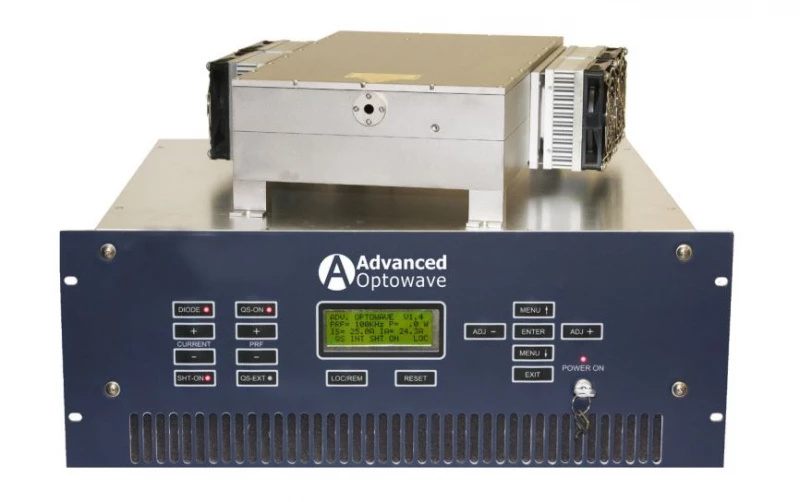

Description
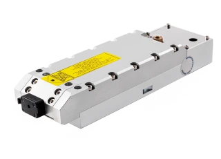
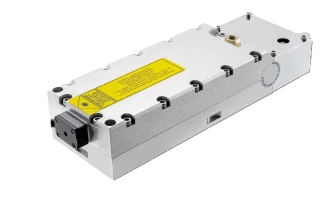
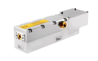
Introducing the AWAVE UV Series, a cutting-edge line of Q-switched TEM00 mode lasers meticulously engineered to meet the rigorous demands of a 24/7 production environment. These industrial lasers are designed to deliver exceptional performance and reliability, making them an ideal choice for various industrial applications. Each system in the AWAVE UV Series comprises a laser head and a laser controller, seamlessly connected by a 2.5-meter umbilical cable. The innovative design places the fiber-coupled pumping diodes within the laser controller, allowing for easy field-replacement and ensuring minimal downtime during maintenance.
The AWAVE UV Series boasts a range of advanced technologies that set it apart in the market. With **innovative end-pumping technology** and **patent pending harmonic conversion technologies**, these lasers provide excellent beam quality, pulse stability, and point stability. The ultra-compact and lightweight design, combined with brand-new focusing optics, ensures precise performance while maintaining a low operational cost. Additionally, the laser head is sealed in a clean room environment to guarantee long-term reliability, making it a robust solution for continuous industrial use.
One of the standout features of the AWAVE UV Series is its versatility in pulse frequencies, ranging from 1-300 kHz, with options extending up to 500 kHz. The series covers an average power range from 100mW to 15W, with pulse energy exceeding 4mJ, catering to a wide array of industrial needs. For applications requiring UV lasers over 40W, the AW-HP Series is available. The AWAVE UV lasers are designed with flexible architectures, allowing for customization to meet specific requirements. With **24/7 proven reliability** and a focus on continuous product improvement, the AWAVE UV Series is a testament to Advanced Optowave's commitment to innovation and quality in industrial laser solutions.
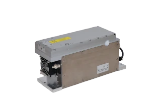
AONano 355-15W-30K ND:YV04 UV Laser
Specifications
| Avg. Power: | 15 W |
|---|---|
| Wavelength: | 355 nm |
| Repetition Rate: | 1 – 300 kHz |
| Spatial Mode (M^2): | 1.2 |
| Pulse Duration: | 15 ns |
| Pulse-to-Pulse Stability (RMS): | 2 % |
| Cooling: | Water-to-Water |
| Pulse Repetition Rate: | Single Shot to 20 kHz |
| Spatial Mode: | TEM00 |
| Beam Roundness: | >90% |
| Pulse Width (ns): | <40ns @1kHz |
| Pulse Width (ns): | <70ns @10kHz |
| Pulse Energy (mJ @ 1kHz): | >0.2mJ |
| Pulse Energy (mJ @ 1kHz): | >0.4mJ |
| Pulse Energy (mJ @ 1kHz): | >0.8mJ |
Got questions about specs? Use the inquiry form to ask.
Features
- Innovative End-Pumping Technology: Provides enhanced performance and efficiency for demanding applications.
- Air-Cooling (Average Power Up to 6W): Efficient cooling system ensures optimal performance and reliability.
- Excellent Beam Quality, Pulse Stability & Point Stability: Delivers precise and consistent results for various industrial applications.
- Patent Pending Harmonic Conversion Technologies: Offers advanced capabilities for superior laser processing.
- Ultra-Compact & Light-Weight: Easy to integrate into existing systems, saving space and reducing weight.
- Brand-New Focusing Optics: Enhances precision and accuracy in laser applications.
- Field-Replaceable Diode: Simplifies maintenance and reduces downtime with easy diode replacement.
- 24/7 Proven Reliability: Engineered for continuous operation in demanding production environments.
- Low Operational Cost: Cost-effective design reduces overall expenses while maintaining high performance.
- Flexible Laser Architectures: Customizable to meet specific requirements beyond standard specifications.
Applications
- Precision Micromachining: Ideal for applications requiring high precision and minimal thermal impact.
- PCB Drilling and Cutting: Suitable for drilling and cutting printed circuit boards with high accuracy.
- Semiconductor Processing: Utilized in wafer dicing and other semiconductor manufacturing processes.
- Medical Device Manufacturing: Enables precise cutting and shaping of medical devices and components.
- Glass and Sapphire Cutting: Effective for cutting and scribing glass and sapphire materials.
- Thin Film Patterning: Used in the patterning of thin films for various electronic applications.
- Solar Cell Processing: Facilitates the processing of solar cells, including edge isolation and drilling.
- LED Manufacturing: Applied in the fabrication and processing of LED components.
- Marking and Engraving: Provides high-quality marking and engraving on a variety of materials.
- Scientific Research: Supports various research applications requiring precise laser technology.
Frequently Asked Questions
What is the AWAVE UV Series laser used for?
What are the features of the AWAVE UV Series laser?
What is the pulse frequency range of the AWAVE UV Series laser?
What is the average power range of the AWAVE UV Series laser?
Does the AWAVE UV Series laser come with a warranty?
Got more questions? Use the RFQ form to ask the supplier directly.
Similar Products


Need pricing for this product? Send a quick inquiry
Your inquiry has been received.
Create an account by adding a password
Why create an account?
- Auto-complete inquiry forms
- View and manage all your past messages
- Save products to your favorites
- Close your account anytime — no hassle