
Description
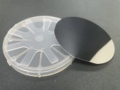
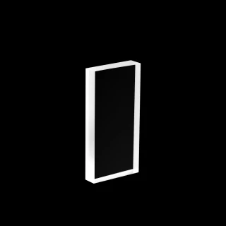
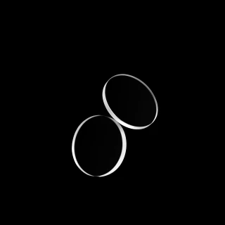
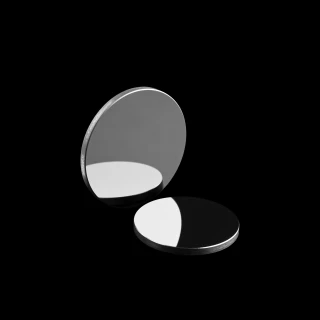
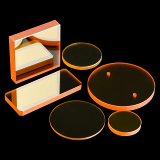
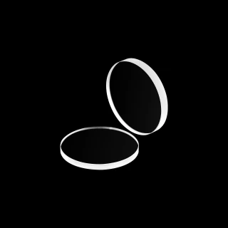
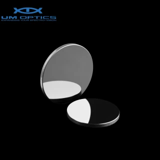
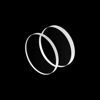
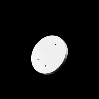
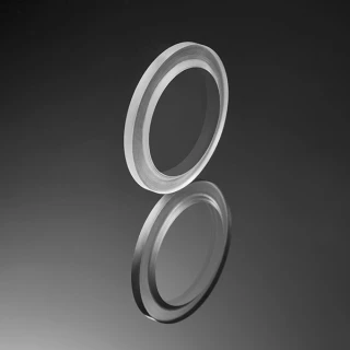
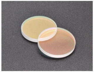
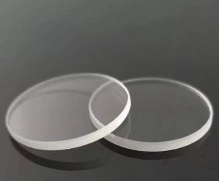
The High-Quality Silicon Wafer is engineered to meet the demanding requirements of the semiconductor and photonics industries. Available in a wide range of sizes and configurations, these wafers are made from CZ (Czochralski) or FZ (Float Zone) silicon, providing exceptional purity and crystal structure. With diameters ranging from 25.4 mm (1 inch) to 304.8 mm (12 inches) and thicknesses from 25 µm to 1 mm, these wafers offer the flexibility needed for various applications. Customers can select from different crystallographic orientations (<100>, <111>, <110>) and conductivity types, including P-type, N-type, or semi-insulating, to match their specific technical needs.
Ideal for manufacturing integrated circuits, sensors, and other photonic devices, these silicon wafers deliver consistent performance, ensuring high yield and reliability in production environments. Whether used for microelectronics or photonic devices, the wafers' customizable dimensions and material purity make them a cornerstone in advanced technological applications.
High-Quality Silicon Wafer for Semiconductor and Photonics Applications
Specifications
| Substrate Material: | Si |
|---|---|
| Antireflection Coating: | Uncoated |
| Diameter: | 304.8 mm |
| Surface Quality: | 20-10 scratch-dig, 40-20 scratch-dig |
| Surface Flatness: | lambda/4 |
| Thickness: | 25 mm |
| Type: | P-Type, N-Type, or Semi-Insulating |
Got questions about specs? Use the inquiry form to ask.
Features
- Wide Range of Sizes: Available in diameters from 25.4 mm (1 inch) to 304.8 mm (12 inches), offering flexibility for various production needs
- Adjustable Thickness: Thicknesses range from 25 µm to 1 mm, suitable for different fabrication processes
- Material Options: Manufactured from high-quality CZ (Czochralski) or FZ (Float Zone) silicon for optimal purity and performance
- Multiple Orientations: Crystallographic orientations include <100>, <111>, and <110>, tailored to specific semiconductor applications
- Versatile Conductivity Types: Available in P-type, N-type, or semi-insulating, ensuring compatibility with various device designs
- High Precision: Designed to meet stringent industry standards for thickness, orientation, and conductivity
Applications
- Semiconductor Manufacturing: Ideal for fabricating integrated circuits, MEMS devices, and other semiconductor components
- Photonics Industry: Perfect for use in the production of sensors, lasers, and other photonic devices
- Research and Development: Essential for advanced research in material sciences, nanotechnology, and microelectronics
- Solar Energy: Applicable for photovoltaic cell production, offering high purity and performance in solar energy applications
- Optoelectronic Devices: Suited for applications requiring precise control of electrical and optical properties in optoelectronic components
Frequently Asked Questions
What material options are available for the silicon wafers?
What sizes are offered for these silicon wafers?
What thickness options are available?
What crystallographic orientations can be selected?
Are the silicon wafers available in different conductivity types?
What are the main applications of these silicon wafers?
How are these wafers suited for the photonics industry?
Can these wafers be customized for specific projects?
What industries commonly use these silicon wafers?
What is the difference between CZ and FZ silicon wafers?
Got more questions? Use the RFQ form to ask the supplier directly.
Similar Products
Need pricing for this product? Send a quick inquiry
Your inquiry has been received.
Create an account by adding a password
Why create an account?
- Auto-complete inquiry forms
- View and manage all your past messages
- Save products to your favorites
- Close your account anytime — no hassle