

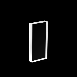
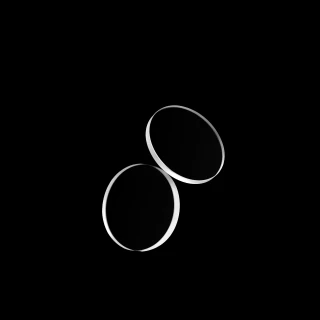
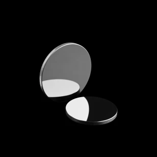
Description
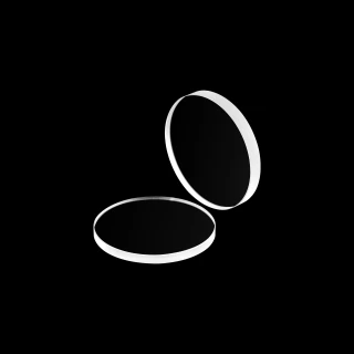
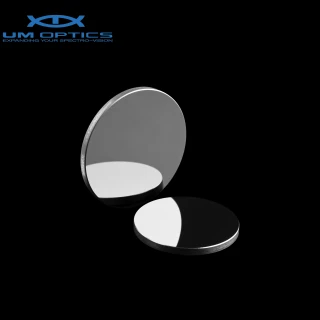
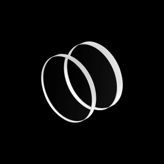
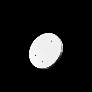
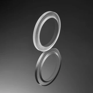
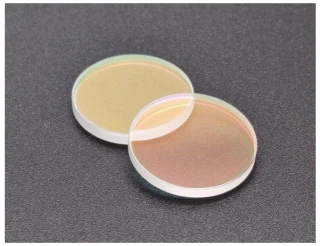
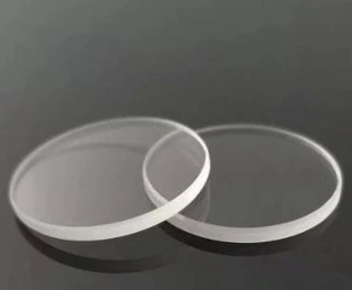
The Sapphire Wafer is an advanced optical component designed specifically for the semiconductor and photonics industries. Manufactured from 99.999% pure AL₂O₃ monocrystalline sapphire, it offers unparalleled durability and performance. With customizable dimensions ranging from 1 inch (25.4 mm) to 8 inches (203.2 mm) and thickness options from 150 µm to 1 mm, it can meet diverse application requirements.
The wafer's C-axis orientation and total thickness variation (TTV) of less than 10 µm ensure exceptional precision and quality. This feature is crucial for high-performance devices, as it minimizes the risk of defects. Additionally, the Sapphire Wafer’s outstanding thermal conductivity and optical clarity make it ideal for demanding applications, including high-power lasers, optics, and integrated circuits. Its ability to withstand extreme environments further enhances its suitability for various technological advancements.
Sapphire Wafer for Semiconductor and Photonics Applications
Specifications
| Substrate Material: | Sapphire |
|---|---|
| Antireflection Coating: | Uncoated |
| Diameter: | 203.2 mm |
| Surface Quality: | 60-40 scratch-dig |
| Surface Flatness: | lambda/4 |
| Thickness: | 1 mm |
| Total Thickness Variation: | Lower than 10 µm |
Got questions about specs? Use the inquiry form to ask.
Features
- High Purity Material: Composed of 99.999% pure AL₂O₃ monocrystalline sapphire for superior optical and thermal performance
- Custom Dimensions: Available in sizes from 1 inch (25.4 mm) to 8 inches (203.2 mm) for versatile applications
- Varied Thickness: Thickness options from 150 µm to 1 mm, accommodating a range of uses
- C-Axis Orientation: Specifically oriented for optimal performance in semiconductor and photonics applications
- Low Total Thickness Variation: TTV of less than 10 µm ensures high-quality substrate characteristics
Applications
- Semiconductor Manufacturing: Ideal for use in the production of semiconductor devices
- Photonics: Suitable for optical devices, including lasers and waveguides
- Optical Coatings: Serves as a substrate for high-performance optical coatings
- Research and Development: Supports experimental setups in advanced material science
Frequently Asked Questions
What is the material of the Sapphire Wafer?
What are the available dimensions?
What is the thickness range?
What orientation does the wafer have?
What is the total thickness variation (TTV)?
What applications are suitable for this wafer?
How does the Sapphire Wafer perform in extreme environments?
Is the Sapphire Wafer coated?
What are the advantages of using sapphire?
Got more questions? Use the RFQ form to ask the supplier directly.
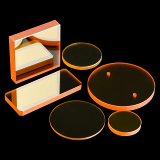
Similar Products
Need pricing for this product? Send a quick inquiry
Your inquiry has been received.
Create an account by adding a password
Why create an account?
- Auto-complete inquiry forms
- View and manage all your past messages
- Save products to your favorites
- Close your account anytime — no hassle