
Description
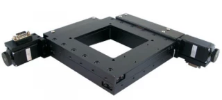
The Carrier Series Stages by MultiFields Technologies are high-performance piezoelectric motion devices designed for precise scanning and positioning in applications such as precision optics and semiconductor characterization.
With their compact shape and powerful performance, these stages offer large-range motion without compromising on power. They ensure accurate positioning, closed-loop control, and customizable solutions for various applications in the field of microscopy and semiconductor characterization.
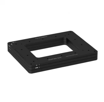
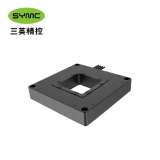
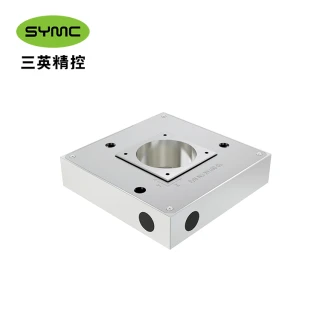
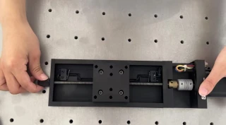
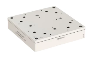
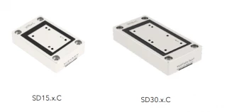
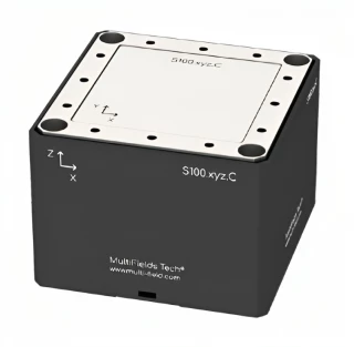
Room Temperature Piezoelectric Carrier Series Stages
Specifications
| Axes Of Motion: | Two |
|---|---|
| Travel Range: | 75 mm |
| Load Capacity (Horizontal): | 2 kg |
| Load Capacity (Vertical): | Not Specified |
| Max Speed: | 20 mm/s |
| Weight: | Not Specified |
| Guiding Mechanism: | Other |
| Voltage Requirement: | DC 24V |
| Full-travel Pitch/yaw: | 0.8 mrad |
| Drive Frequency (Max): | 20 kHz |
| Min. Step: | ~ 30 nm |
| Operating Temperature: | 10 – 40 °C |
| Cables & Connectors: | Standard shielded cable D-Sub 9 Connector |
| Main Material: | Aluminum alloy |
| Effective Perforation: | 85 mm × 65 mm |
| Required Installation Space: | 325 mm × 250 mm |
| Dimensions: | 250 mm × 200 mm × 30 mm |
Got questions about specs? Use the inquiry form to ask.
Features
- XY-directional range of 75 mm × 50 mm for versatile positioning
- Smallest step size of about 20 nm for high-resolution control
- Maximum velocity of 20 mm/s for fast and efficient operation
- Closed-loop sensing with 100 nm / 10 nm spatial resolution for precise feedback
- Guaranteed through-hole of 85 mm × 65 mm for a full range of motion
- Supports non-magnetic (.NM) and ultra-high vacuum (.UHV) options for enhanced versatility
- Main body made of aluminum alloy with hard oxide blackened coating for durability
Applications
- Precision optics alignment and characterization
- Semiconductor wafer inspection and testing
- Microscopy and imaging systems
- Metrology and measurement devices
- Nanotechnology research and development
- MEMS (Micro-Electro-Mechanical Systems) testing
- Material science research
- Super-resolution optical microscopy
Frequently Asked Questions
What are the dimensions of the XY-directional range for positioning?
What is the smallest step size for high-resolution control?
What is the maximum velocity for operation?
What is the spatial resolution for closed-loop sensing?
What are the options for enhanced versatility?
Got more questions? Use the RFQ form to ask the supplier directly.
Similar Products


Need pricing for this product? Send a quick inquiry
Your inquiry has been received.
Create an account by adding a password
Why create an account?
- Auto-complete inquiry forms
- View and manage all your past messages
- Save products to your favorites
- Close your account anytime — no hassle