


Description
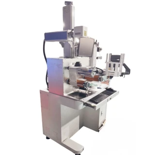
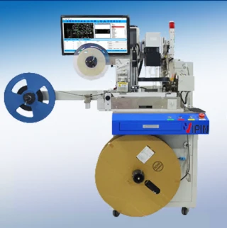
VIPIN 4545ATN Automatic PCB Laser Marking Machine UV Fiber CO2
The VIPIN-4545ATN Automatic PCB Laser Marking Machine is a high‑performance solution engineered for fast, precise, and permanent identification of printed circuit boards in modern SMT and electronic assembly lines. Designed to replace conventional inkjet and label printing, this system delivers maintenance‑free, consumable‑free marking with exceptionally fine resolution and superior contrast on a wide range of PCB substrates. With a generous 450 mm × 450 mm marking area, it supports both small panels and large multi‑up PCB arrays, making it suitable for high‑volume production environments in consumer electronics, automotive, telecommunications, industrial control, and medical device manufacturing.
Compared with traditional printing methods, PCB laser marking offers a clean and reliable way to encode boards with barcodes, 2D DataMatrix, and QR codes, as well as alphanumeric text and logos. The VIPIN-4545ATN uses a high‑speed galvanometer scanning system to achieve marking speeds up to 7000 mm/s while maintaining excellent accuracy and repeatability. Its configuration supports multiple laser sources — including UV, fiber, green, and CO2 — enabling optimized marking performance for different PCB materials, solder masks, and coatings. This flexibility ensures clear, permanent marks without damaging delicate circuits or affecting downstream processes such as soldering, conformal coating, or reflow.
Engineered specifically for inline integration, the VIPIN 4545ATN Automatic PCB Laser Marking Machine can be installed at the front end of an SMT line, where incoming bare boards or assembled PCBs are automatically marked before entering subsequent production stages. It can be used in both inline and offline modes and is compatible with standard loaders and unloaders, allowing seamless integration into existing production flows. Its conveyor system is designed to accommodate PCB sizes from 50 mm × 50 mm up to 450 mm × 450 mm, with typical board thicknesses from 0.5 mm to 3 mm. Optional flip‑marking capability can be configured when both sides of the PCB require identification.
For factories implementing traceability and smart manufacturing, the VIPIN-4545ATN supports MES connectivity, enabling automatic data exchange between the laser marker and the production management system. Circuit board puzzle (panel) handling is fully supported, so multiple boards in a panel can be recognized and marked individually with unique serials or codes. With optional CCD automatic code reading and QR code grade recognition, the system can verify mark quality in real time, ensure readability, and reduce the risk of traceability failures. This closed‑loop verification is particularly valuable in industries that must comply with strict quality, regulatory, and audit requirements.
The machine is designed for stable, long‑term operation on the production floor. A CO2 laser configuration with 10 W power and a wavelength around 10.6 µm provides a typical service life of at least 20,000 hours, significantly reducing downtime and total cost of ownership. Fine spot diameter and tightly controlled power fluctuation deliver consistent marking depth and contrast across large batches. High positioning accuracy (on the order of ±0.05 mm) and repeatability (around ±0.02 mm) ensure that codes are placed precisely within the designated marking windows, even on densely populated or miniaturized PCBs.
To support diverse production teams and maintain process security, the VIPIN-4545ATN includes multi‑level permission management with separate roles for administrators, technicians, and operators. Its software interface is designed for ease of use, enabling quick setup of new products, mark layouts, and panel formats without extensive programming knowledge. Combined with the option to choose the most suitable laser source for each application (UV for high‑contrast, low‑thermal marking; fiber for metals and certain components; green and CO2 for specific PCB substrates), the system delivers a scalable, future‑proof platform for PCB identification and full lifecycle traceability.
Automatic PCB Laser Marking Machine UV Fiber CO2
Specifications
| Work Area X: | 450 mm |
|---|---|
| Work Area Y: | 450 mm |
| Beam Delivery: | Galvo |
| Laser Source: | Fiber |
| Laser Output Power: | 5 W |
| Laser Wavelength: | 532 nm (green) |
| Marking Speed: | 7000 mm/sec |
| Voltage Requirement: | 220V - 50Hz |
| Materials: | Stainless Steel, Steel/Iron, Steel Alloy, Aluminum, Anodized Aluminum, Brass, Copper, Gold, Silver, Nickel, Titanium, Platinum, Glass, Plastic, Wood, Paper, Textile, Granite, Marble, Nylon, Acrylic, Plexiglass |
| Air Assist: | Included |
| Fume Extraction Unit: | Included |
| Safety Enclosure: | Included |
| Laser Type: | CO2 Synrad 10W (Optional: UV, Green & Fiber Laser) |
| Laser Wave Length: | 10640nm |
| Laser Power: | 10W |
| Marking Area: | 450mm×450mm |
| Marking Speed: | Max: 7000mm/s |
| Marking Position Accuracy: | ±0.05mm (Optional) |
| Repeatability: | ±0.02mm |
| Applicable PCB Size: | 50mm×50mm-450mm×450mm |
| PCB Thickness: | 0.5mm-3mm (Optional) |
| Upper Surface Height: | <25mm (Optional) |
| PCB Lower Surface Height: | <25mm |
Got questions about specs? Use the inquiry form to ask.
 Download Data Sheet

Features
- Versatile Laser Sources (UV / Fiber / Green / CO₂) – Configurable with UV, fiber, green, or CO₂ lasers to match diverse PCB materials and marking requirements, from FR4 and ceramics to coated and flexible boards.
- High‑Precision, High‑Speed PCB Laser Marking – Up to 7000 mm/s marking speed with a high‑speed galvanometer and ±0.05 mm positioning accuracy (optional) and ±0.02 mm repeatability, ideal for fine QR codes, barcodes, and micro text.
- Large 450 × 450 mm Marking Area – Generous working field of 450 mm × 450 mm for single large PCBs or multi‑up panelized boards, improving throughput and reducing handling steps.
- Wide PCB Size and Thickness Compatibility – Supports PCB sizes from 50 × 50 mm to 450 × 450 mm and thicknesses from 0.5–3 mm (optional ranges), with upper and lower component heights up to 25 mm, suitable for most SMT and assembly lines.
- Automatic CCD Code Reading & Verification – Integrated CCD camera for automatic code reading and QR code grade recognition (optional) ensures accurate content, orientation compensation, and traceability validation directly after marking.
- Inline & Offline Operation for Flexible Integration – Can be used as a stand‑alone offline system or fully inline within SMT and PCB production lines, allowing staged implementation or direct connection to existing equipment.
- Seamless MES Connectivity – Supports MES interconnection for automatic job loading, real‑time data upload, serial number management, and full process traceability, meeting Industry 4.0 and smart factory requirements.
- Loader & Unloader Compatibility – Easily integrated with automatic PCB loader and unloader modules or directly inserted into the SMT line, minimizing manual handling and improving production efficiency.
- Flip Marking Capability (Optional) – Optional flip marking function allows marking on both sides of the PCB without manual flipping, ideal for double‑sided identification and complex traceability schemes.
- Consumable‑Free, Low‑Maintenance Process – Laser marking eliminates the need for inks, labels, or solvents, resulting in no consumables, minimal maintenance, and a cleaner, more environmentally friendly process compared with conventional printing.
- Long‑Life CO₂ Laser Source – CO₂ configuration with U.S.‑made laser (e.g., Synrad‑class) offers ≥ 20,000 hours lifespan, 10 W power, 10.6 μm wavelength, stable power fluctuation < 3%, and approx. 0.13 mm spot diameter for sharp, permanent marks.
- High‑Quality 1D & 2D Code Marking – Capable of marking min. 3.0 × 3.0 mm QR codes, barcodes, Data Matrix, alphanumeric text, logos, and graphics with excellent legibility for downstream scanners and AOI systems.
- User‑Friendly PCB Puzzle Function & Software – Dedicated PCB “puzzle” (panelization) function and simple, intuitive software streamline job setup, automatic field segmentation, and quick format changes, reducing programming time.
- Multi‑Level Permission Management – Built‑in administrator / technician / operator permission levels provide secure access control, protecting parameters, recipes, and MES communication settings from unauthorized changes.
- Stable, Industrial‑Grade Performance – Designed for 24/7 production with robust mechanical structure, precision motion, and high‑speed galvanometer scanning to ensure consistent output in demanding electronic manufacturing environments.
- Clean, Non‑Contact Marking – Non‑contact laser marking avoids mechanical stress or contamination on PCBs, preserving pad quality and surface integrity, and reducing rework or scrap.
- Ideal for SMT, EMS, and PCB Fabrication – Optimized for PCB manufacturers, EMS providers, and SMT production lines requiring reliable product identification, serialization, lot coding, and lifetime traceability.
Applications
- PCB Traceability and Identification – Permanent laser marking of 1D/2D barcodes, QR codes, DataMatrix codes, serial numbers, and batch IDs on single PCBs and panelized circuit boards for end-to-end traceability in electronics manufacturing.
- SMT and PCBA Production Lines – Inline and offline marking of printed circuit boards before and after SMT placement, reflow soldering, and wave soldering, with seamless integration to loaders, unloaders, and conveyors.
- MES and Industry 4.0 Integration – Real‑time data exchange with MES/ERP systems for automatic work‑order assignment, production tracking, quality feedback, and intelligent process control in fully digital factories.
- Consumer Electronics Manufacturing – High‑precision marking of PCB assemblies used in smartphones, tablets, laptops, wearables, game consoles, smart home devices, and other high‑volume consumer products.
- Automotive Electronics and EV Systems – Durable marking of control units, BMS PCBs, ADAS modules, infotainment boards, inverters, chargers, and sensor PCBs where high reliability and anti‑counterfeiting identification are critical.
- Industrial Control and Power Electronics – Coding of PCBs used in PLCs, industrial drives, inverters, servo controllers, power supplies, and industrial IoT gateways exposed to harsh environments where ink printing is not reliable.
- Medical Device Electronics – Non‑contact, low‑contamination marking of circuit boards for diagnostic equipment, patient monitoring, imaging systems, and portable medical devices, supporting UDI and strict traceability requirements.
- Telecommunications and Networking Hardware – Marking of PCBs for routers, switches, base stations, optical transceivers, and 5G infrastructure with high‑contrast QR codes and alphanumeric IDs for fast scanning and maintenance.
- Aerospace and Defense Electronics – Permanent, high‑accuracy marking of mission‑critical PCBs where resistance to abrasion, solvents, and extreme temperatures is required and mechanical or ink methods are not acceptable.
- LED Lighting and Display Modules – Laser coding of LED driver boards, strip light PCBs, display backlight boards, and signage modules without damaging sensitive components or affecting optical performance.
- Home Appliances and White Goods – Traceability marking on PCBs used in refrigerators, washing machines, air conditioners, kitchen appliances, and smart appliances to reduce warranty costs and improve after‑sales service tracking.
- High‑Density and Fine‑Pitch PCBs – Micro‑sized code and text marking on HDI, rigid‑flex, and fine‑pitch PCBs where limited space and small pad spacing demand very small spot size and high positioning accuracy.
- Rigid, Flexible and Rigid‑Flex PCB Marking – Contact‑free laser marking on a wide range of PCB substrates, including FR‑4, polyimide, flexible circuits, and composite materials using UV, green, fiber, or CO₂ laser configurations.
- Panelized PCB (Array) Marking – Use of automatic panel (puzzle) function to mark multiple boards in a panel with unique or shared codes, optimizing cycle time and ensuring consistent marking across the entire array.
- Marking on Solder Mask and Bare Copper – High‑contrast codes and logos on green, black, blue, white, and other solder mask colors as well as bare copper areas without additional consumables or pre‑treatment.
- Logo, Text and Graphic Marking – Permanent branding with company logos, regulatory symbols, polarity marks, functional labels, and assembly guides directly on the PCB surface.
- Anti‑Counterfeiting and Brand Protection – Marking of unique QR codes, encrypted DataMatrix codes, and invisible micro‑codes on PCBs to protect high‑value electronics from counterfeiting and grey‑market diversion.
- Lot, Date, and Process Code Marking – Automated printing of production date, lot number, line number, shift data, and process parameters for quality control and rapid recall management.
- Repair, Rework and After‑Sales Tracking – Clear and durable identification of PCBs through multiple repair and rework cycles, enabling traceability of service history and failure analysis.
- Prototype and Small‑Batch PCB Production – Fast, flexible marking for R&D labs, prototyping centers, and small‑batch EMS production where frequent design changes make conventional printing methods impractical.
Frequently Asked Questions
What is the Automatic PCB Laser Marking Machine UV Fiber CO2 and what is it used for?
What laser types are available and which one should I choose for my PCB application?
What are the marking area and PCB size capabilities of the Automatic PCB Laser Marking Machine UV Fiber CO2?
How accurate and fast is the VIPIN-4545ATN PCB laser marking machine?
Can the VIPIN-4545ATN be integrated into an SMT production line and MES system?
What automation and software features does this PCB laser marker include?
What are the maintenance and operating cost advantages compared to traditional PCB printing or labeling?
Got more questions? Use the inquiry form to ask the supplier directly.
Similar Products


Your inquiry has been received.
Create an account by adding a password
Why create an account?
- Auto-complete inquiry forms
- View and manage all your past messages
- Save products to your favorites
- Close your account anytime — no hassle