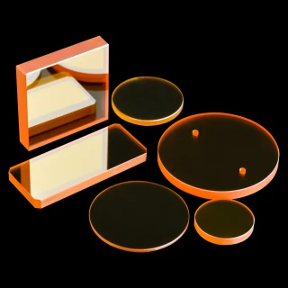
Description
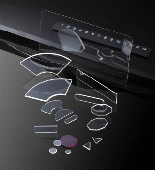
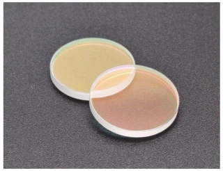
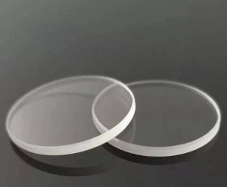
Our sapphire substrates are designed for high-end applications that demand exceptional durability, optical clarity, and thermal stability. Utilizing advanced micro-machining techniques, we offer substrates in various shapes and sizes, tailored to meet the precise needs of our customers. From LED packaging to scientific research, our sapphire substrates are crafted to deliver superior performance and reliability.
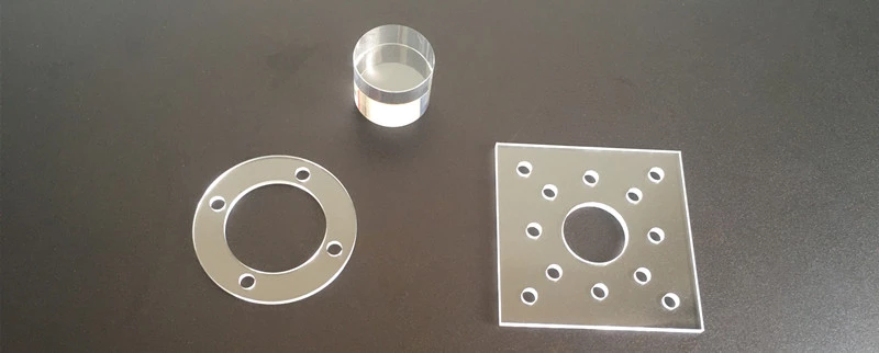
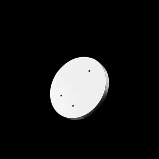
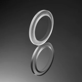
High-Precision Sapphire Substrates for LED Packaging and Micro Machining
Specifications
| Substrate Material: | Sapphire |
|---|---|
| Antireflection Coating: | Uncoated |
| Diameter: | 0.01 mm |
| Surface Quality: | Not Specified |
| Surface Flatness: | Other |
| Tolerance: | 5~20 micrometers |
Got questions about specs? Use the inquiry form to ask.
Features
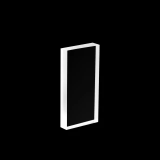
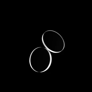
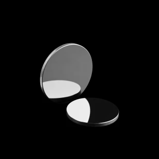
- High-purity sapphire material for excellent optical clarity and durability
- Custom shapes and sizes including circles, triangles, rectangles, hexagons, and polygons
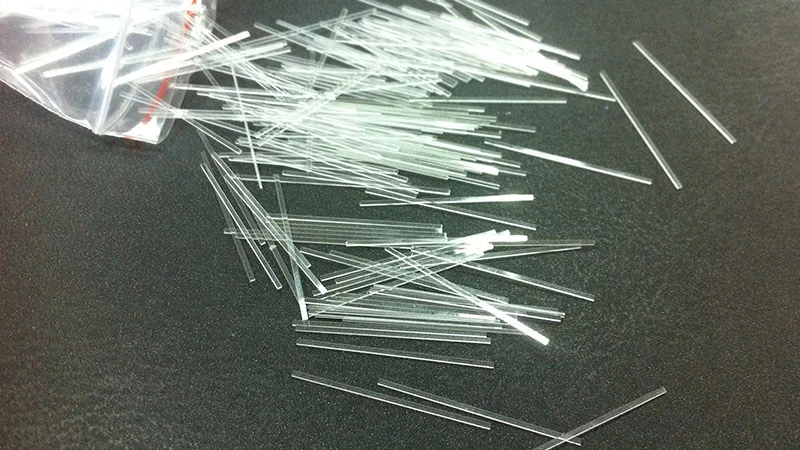
- Min feature size capability of 0.01mm
- Tight tolerance levels ranging from 5 to 20 micrometers
- Superior cutting and sidewall polishing techniques to prevent chipping
- Available in different polishing requirements to suit various applications
Applications
- LED packaging
- Microfluidic devices
- Optical instruments
- Watch assemblies
- High-precision sensors
- Scientific research equipment
Frequently Asked Questions
What are sapphire substrates?
Sapphire substrates are thin slices or wafers of high-purity sapphire material used in various high-end applications. They are known for their exceptional optical clarity, durability, and thermal stability.
What are the main applications of sapphire substrates?
Sapphire substrates are widely used in LED packaging, microfluidic devices, optical instruments, watch assemblies, high-precision sensors, and scientific research equipment.
Can you customize the shape and size of the sapphire substrates?
Yes, we offer custom shapes and sizes, including circles, triangles, rectangles, hexagons, polygons, or any shape as per your CAD designs.
What is the minimum feature size you can achieve?
Our advanced micro-machining techniques allow us to achieve a minimum feature size of 0.01mm.
What tolerance levels do you offer?
We offer tight tolerance levels ranging from 5 to 20 micrometers, depending on the dimension and application requirements.
What cutting technologies do you use for sapphire substrates?
We utilize a combination of precision CNC, laser cutting, and chemical etching technologies to ensure high precision and quality in our sapphire substrates.
What polishing quality can I expect from your sapphire substrates?
Our sapphire substrates undergo superior cutting and sidewall polishing techniques to prevent chipping and ensure excellent edge quality.
Do you provide different polishing requirements?
Yes, we offer sapphire wafers with different polishing requirements to suit various applications.
Got more questions? Use the RFQ form to ask the supplier directly.
Similar Products
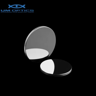
Sapphire Optical Flat Windows
CSOC
Optical UV Grade Calcium Fluoride Monocrystalline CaF2 Window for Precision Ultraviolet Optical Systems
Henan UM Optics Ltd
Low Fluorescence Optical Raman Grade CaF2 Calcium Fluoride Window for Precision Optics
Henan UM Optics Ltd
High Precision Polished Chalcogenide Glass IRG206 Windows
Henan UM Optics Ltd
Custom High Transmission Infrared CVD Zinc Selenide ZnSe Window for IR Imaging & Spectroscopy
Henan UM Optics Ltd
Factory Custom Optical Potassium Bromide KBr Windows for Infrared Imaging Systems and IR Laser Optical Setups
Henan UM Optics Ltd
Custom Optical Germanium Window Ge Infrared Protective windows with AR/DLC Coating
Henan UM Optics Ltd
Factory Custom High Transmittance Optical N-BK7 Glass Window
Henan UM Optics Ltd
Custom High Precision Optical Polished P Type Silicon Drilled Windows
Henan UM Optics Ltd
Custom Optical Monocrystalline Infrared CaF2 Calcium Fluoride Round Step Window
Henan UM Optics Ltd
High-Precision Laser Windows for Visible to Infrared Wavelengths
CRYSTECH Inc.
High-Precision Optical Windows | Durable Protective Barriers for Sensors
Langjie-optics Inc
Need pricing for this product? Send a quick inquiry
Thank You!
Your inquiry has been received.
Create an account by adding a password
Why create an account?
- Auto-complete inquiry forms
- View and manage all your past messages
- Save products to your favorites
- Close your account anytime — no hassle