


Description
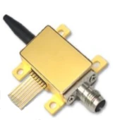
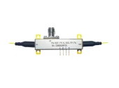
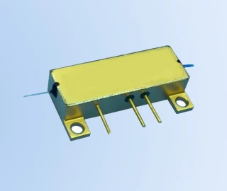
This thin film lithium niobate (TFLN) intensity modulator is a high‑performance electro‑optic device engineered for next‑generation high‑speed optical transmission. Designed around an advanced thin‑film LiNbO₃ platform and precision fiber–chip coupling, it delivers ultra‑efficient electro‑optical conversion with significantly reduced half‑wave voltage compared with traditional bulk lithium niobate modulators. The compact package integrates thermo‑optic bias control for long‑term stability, making it an excellent choice for demanding applications in high‑speed digital optical communications, microwave photonics, coherent transmission systems, and research testbeds.
Optimized for both C‑band (~1550 nm) and O‑band (~1310 nm) operation, this modulator supports 3 dB electro‑optic bandwidths up to 40 GHz, enabling advanced modulation formats and very high symbol rates. Insertion loss is typically 4.5 dB with a maximum of 5.5 dB, competitive with state‑of‑the‑art TFLN and conventional LiNbO₃ modulators used in metro, long‑haul, and data center interconnect links. An extinction ratio of ≥20 dB (with higher extinction ratios above 25 dB available on customization) supports clean on/off modulation with low residual optical carrier, suitable for high‑contrast intensity modulation and precise amplitude shaping.
The device is available in 20 GHz and 40 GHz RF bandwidth options, giving designers flexibility for both cost‑sensitive and ultra‑high‑speed systems. The 3 dB electro‑optic bandwidth is typically 20 GHz for the 20 GHz version and 40 GHz for the 40 GHz version, starting from 2 GHz, which matches or exceeds many comparable intensity modulators used for 10G to 64G‑baud and beyond. The RF half‑wave voltage (Vπ) is impressively low: for C‑band operation, typical values are around 2.5 V (maximum 3.0 V) for the 20 GHz class device and 3.0 V (maximum 3.5 V) for the 40 GHz class device. In O‑band, Vπ is even lower, with a typical value of 2.0 V and a maximum of 2.5 V. This low drive voltage allows direct interfacing with modern high‑speed drivers and significantly reduces system power consumption and driver complexity.
To ensure stable operating conditions and drift‑free biasing, the modulator incorporates thermo‑optical bias control. A dedicated heater structure provides a bias half‑wave power (Pπ) of ≤50 mW, enabling precise and efficient setting of the operating point (for example, at quadrature) without requiring large electrical bias voltages. This thermal bias mechanism improves long‑term stability versus environmental temperature changes and mechanical fluctuations, which is crucial in field‑deployed systems and long‑duration laboratory measurements. RF return loss is specified better than –10 dB from 2 GHz to 40 GHz, supporting good impedance matching and minimizing reflections in high‑frequency RF chains.
The optical interface is optimized for single‑mode fiber coupling in the O‑band and C‑band, with optical return loss of ≤ –27 dB to reduce back‑reflection and interference. The low insertion loss, together with high extinction ratio, offers an excellent optical signal‑to‑noise ratio for intensity‑modulated direct detection and microwave photonics links. The small device footprint relative to traditional bulk LiNbO₃ modulators simplifies integration in compact transceiver modules, photonic subsystems, and benchtop experimental setups. It is well suited for backbone communication networks, analog optical links, RF‑over‑fiber distribution, and modulation formats ranging from simple on–off keying to advanced multi‑level amplitude schemes used in modern optical interconnects.
In terms of environmental robustness, the thin film lithium niobate intensity modulator is specified for an operating temperature range from –20 °C to +70 °C, making it appropriate for both controlled laboratory environments and many field‑deployed communication systems. Storage temperatures from –40 °C to +85 °C and wide humidity tolerance (5% to 90% non‑condensing) support safe logistics and long‑term inventory management. The damage thresholds are clearly defined to protect the device: RF input power is limited to 18 dBm, RF input swing to ±2.5 Vpp, RMS RF voltage to 1.78 Vrms, optical input power to 20 dBm, and heater bias to 4.5 V and 50 mA. Adhering to these limits ensures reliable long‑term performance comparable with other high‑end intensity modulators used in advanced optical test and measurement, system prototyping, and commercial communication equipment.
Overall, this thin film lithium niobate 20 GHz / 40 GHz intensity modulator combines low Vπ, wide RF bandwidth, low insertion loss, and integrated thermo‑optic bias control in a compact package.
Thin Film Lithium Niobate Intensity Modulator 20GHz 40GHz C Band O Band
Specifications
| Aperture Diameter: | Not Specified |
|---|---|
| Peak Optical Power Density: | Not Specified |
| Wavelength Range: | 1530 – 1565 nm |
| Transmission: | Not Specified |
| Extinction Ratio: | Not Specified |
| Operating Wavelength Typical (C-band): | ~1550 nm |
| Additional Option - Operating Wavelength (O-band): | ~1310 nm |
| Optical Extinction Ratio (DC): | ≥20 dB |
| Optical Return Loss: | ≤-27 dB |
| Optical Insertion Loss (typical): | 4.5 dB |
| Optical Insertion Loss (maximum): | 5.5 dB |
| 3 DB Electro-optical Bandwidth (X1:2, C-band): | 18–20 GHz |
| 3 DB Electro-optical Bandwidth (X1:4, C-band): | 36–40 GHz |
| 3 DB Electro-optical Bandwidth (X1:2, O-band): | 18–20 GHz |
| 3 DB Electro-optical Bandwidth (X1:4, O-band): | 36–40 GHz |
| RF Half-wave Voltage @50 KHz (C-band, X3:5): | Typ 2.5 V, Max 3.0 V |
| RF Half-wave Voltage @50 KHz (C-band, X3:6): | Typ 3.0 V, Max 3.5 V |
| RF Half-wave Voltage @50 KHz (O-band, X3:4): | Typ 2.0 V, Max 2.5 V |
| Heat-modulated Bias Half-wave Power: | ≤50 mW |
| RF Return Loss (2 GHz To 40 GHz): | ≤-10 dB |
| Operating Temperature: | -20 to 70 °C |
| RF Input Power Damage Threshold: | ≤18 dBm |
| RF Input Swing Voltage Damage Threshold: | ±2.5 Vpp |
| RF Input RMS Voltage Damage Threshold: | ≤1.78 Vrms |
| Optical Input Power Damage Threshold: | ≤20 dBm |
| Thermo-tuned Bias Voltage Damage Threshold: | ≤4.5 V |
| Hot Tuning Bias Current Damage Threshold: | ≤50 mA |
| Storage Temperature: | -40 to 85 °C |
| Relative Humidity (no Condensation): | 5–90 % RH |
Got questions about specs? Use the inquiry form to ask.
 Download Data Sheet

Features
- Ultra‑High RF Bandwidth up to 40 GHz
Delivers wide 3 dB electro‑optical bandwidth (typ. 20 GHz / 40 GHz options) for high‑speed digital optical communication, advanced microwave photonics, 5G/6G research, and high‑frequency test systems. - Low Half‑Wave Voltage (Vπ) for High Modulation Efficiency
Features low RF half‑wave voltage (typ. 2.0–3.0 V depending on band and configuration), enabling efficient electro‑optic conversion, reduced drive power, and simplified RF driver requirements compared to conventional bulk LiNbO₃ modulators. - Thin‑Film Lithium Niobate Platform
Based on advanced thin‑film LiNbO₃ technology to achieve higher electro‑optic efficiency, stronger light–RF confinement, and lower power consumption in a significantly more compact form factor than traditional lithium niobate crystal devices. - Wide Operating Wavelength Options (C‑Band & O‑Band)
Supports telecom‑grade wavelength windows with versions optimized for ~1550 nm (C‑band) and ~1310 nm (O‑band), making the device suitable for backbone networks, metro networks, data‑center interconnects, and research setups across standard fiber‑optic bands. - High Extinction Ratio for Clean Signal Modulation
Provides a typical optical extinction ratio ≥ 20 dB, with customizable high‑extinction options > 25 dB, ensuring excellent ON/OFF contrast for advanced modulation formats and low crosstalk in coherent and intensity‑modulated links. - Low Optical Insertion Loss
Utilizes precision optical coupling and packaging for typical insertion loss around 4.5 dB (max. 5.5 dB), improving link budget and system reach, especially important in long‑haul and high‑capacity photonic networks. - Integrated Thermo‑Optic Bias Control
Built‑in thermo‑optic bias (heater) enables stable operating point control with half‑wave heater power ≤ 50 mW, minimizing drift and ensuring long‑term DC bias stability for demanding laboratory, network, and field applications. - Compact, Small‑Footprint Device Package
Thin‑film design combined with high‑precision packaging yields a small device size, ideal for dense instrumentation, OEM integration, multi‑channel systems, and space‑constrained photonic platforms. - Optimized RF Performance and Matching
RF return loss S11 ≤ −10 dB from 2 GHz to 40 GHz provides good impedance matching to 50‑ohm RF drivers and measurement equipment, reducing reflections, preserving signal integrity, and simplifying high‑frequency system design. - Robust Optical Return Loss Performance
Optical return loss ≤ −27 dB reduces back‑reflections into lasers and upstream optics, improving source stability and minimizing noise in coherent and intensity‑modulated systems. - Broad Operating Temperature Range
Designed for reliable operation from −20 °C to +70 °C, supporting use in both controlled laboratory environments and more demanding field or equipment‑rack conditions. - Carefully Defined Damage Thresholds
Specified limits for RF input power, RF voltage swing, optical input power, and heater drive (voltage/current) help prevent irreversible damage, supporting safe integration into high‑power and high‑speed testbeds. - Ideal for High‑Speed Optical Communication Systems
Tailored for intensity modulation in 10G to 64G+ and beyond, PAM‑4, NRZ, and advanced modulation formats in C‑band and O‑band fiber‑optic links used in backbone networks, metro networks, and data‑center connectivity. - Excellent Choice for Microwave Photonics & RF‑over‑Fiber
High bandwidth, low Vπ, and thin‑film platform make this modulator well‑suited for RF‑over‑fiber, radar link distribution, phased‑array antenna beamforming, analog photonic links, and other microwave photonic applications. - Research‑Grade Stability and Repeatability
High stability, bias control, and well‑characterized electro‑optic behavior make the device attractive for university and industrial R&D in integrated photonics, quantum communication experiments (intensity control), and high‑speed optical signal processing. - Independently Developed with Proprietary IP
The modulator is independently developed with full proprietary intellectual property, offering long‑term product support, customization potential, and supply‑chain security for OEM and system‑level customers.
Applications
- High‑speed digital optical communication systems – Use in 20–40 GHz intensity modulation for 100G/200G/400G and beyond coherent and direct‑detect links in C‑band (~1550 nm) and O‑band (~1310 nm). Ideal for data center interconnects, short‑reach and long‑haul metro networks where low half‑wave voltage and low insertion loss improve link budgets.
- Backbone and metro fiber‑optic communication networks – Deployment in high‑capacity DWDM/ CWDM backbone networks and metro rings to generate stable, high‑extinction optical signals. The low Vπ and high electro‑optic bandwidth help maximize spectral efficiency and support advanced modulation formats (NRZ, PAM4, QPSK, QAM).
- Microwave photonics links – Optical modulation of RF and microwave signals up to 40 GHz for radar remoting, antenna remoting, and low‑loss RF signal distribution over fiber. Thin‑film LiNbO₃ enables low drive voltages and improved linearity compared with traditional bulk LiNbO₃ modulators.
- 5G/6G fronthaul and backhaul over fiber – Conversion of high‑frequency wireless signals to the optical domain for C‑RAN, distributed antenna systems, and small‑cell backhaul. The broad RF bandwidth and low noise help support mmWave and sub‑THz research links using analog radio‑over‑fiber (RoF) architectures.
- High‑speed test and measurement systems – Use as a calibrated optical intensity modulator in photonic testbeds, BERT setups, optical sampling oscilloscopes, and component characterization systems for validating high‑speed transceivers, drivers, and photodiodes.
- Optical arbitrary waveform generation (OAWG) – Building block in systems that synthesize tailored optical pulse trains and complex intensity envelopes for coherent control, optical metrology, and advanced communication formats.
- Pulsed laser modulation and gating – Intensity modulation of narrow‑linewidth or mode‑locked lasers around 1310 nm and 1550 nm for pulse carving, gain‑switched or externally‑modulated laser sources, optical packet generation, and optical time‑division multiplexing (OTDM).
- Secure optical communication and quantum‑related experiments – Precise intensity control for quantum key distribution (QKD) decoy states, quantum channel characterization, and classical–quantum co‑existence experiments, where high extinction ratio and stable thermo‑optic bias are essential.
- All‑optical signal processing and photonic computing – Front‑end modulator for neuromorphic photonics, optical computing accelerators, and optical AI engines that require high‑speed, low‑power electro‑optic interfaces on thin‑film LiNbO₃ platforms.
- Optical sensing and lidar modulation – Generation of high‑bandwidth intensity‑modulated light for coherent FMCW lidar, fiber‑optic sensing (Φ‑OTDR, BOTDA/BOTDR) and interferometric measurement systems, where compact size and high stability are critical.
- Analog photonic signal processing – Use in RF photonic filters, phase‑controlled links, and analog‑to‑digital conversion front ends based on photonic techniques. The low Vπ and wide 3 dB bandwidth enable linear, wide‑dynamic‑range RF‑over‑fiber links.
- Research and development in integrated photonics – Ideal platform component for university and industrial R&D labs working on thin‑film LiNbO₃ integrated circuits, electro‑optic frequency combs, and next‑generation modulators with ultra‑low drive voltages.
- Coherent optical system prototyping – Use as the intensity modulator in coherent transmitters for developing and testing coherent detection algorithms, DSP, and advanced FEC schemes at 20–40 GHz symbol rates.
- Optical clock distribution and timing systems – Stable intensity modulation of reference lasers for timing distribution over fiber in large‑scale facilities (accelerators, observatories, data centers), benefiting from the device’s thermo‑optic bias control and high reliability over −20 °C to 70 °C.
- Education and training platforms – Integration into advanced photonics training kits and university laboratories to demonstrate electro‑optic modulation principles, microwave photonics, and high‑speed optical communication techniques using state‑of‑the‑art thin‑film LiNbO₃ technology.
Frequently Asked Questions
What is the Thin Film Lithium Niobate 20 GHz / 40 GHz Intensity Modulator and what applications is it designed for?
What are the key optical and electrical specifications of this 20 GHz / 40 GHz lithium niobate intensity modulator?
How does the thermo‑optic bias control work and how should I set the bias point?
What are the RF and optical damage thresholds and how can I avoid damaging the modulator?
What is the difference between the C‑band and O‑band versions and how do I choose the right one?
How should I connect and drive the RF port of this 20/40 GHz thin‑film lithium niobate modulator?
Can this thin‑film lithium niobate intensity modulator be customized (extinction ratio, wavelength, bandwidth, packaging)?
Got more questions? Use the inquiry form to ask the supplier directly.
Similar Products



Your inquiry has been received.
Create an account by adding a password
Why create an account?
- Auto-complete inquiry forms
- View and manage all your past messages
- Save products to your favorites
- Close your account anytime — no hassle