


Description
Supplier of Stress Testing Instruments
In the intricate world of electronics manufacturing, ensuring the reliability and durability of printed circuit board assemblies (PCBAs) is paramount. As a leading supplier of stress testing instruments, we provide comprehensive solutions for PCBA strain measurement. Our tools are designed to help manufacturers identify and mitigate mechanical stresses that can lead to component failure, ensuring the longevity and performance of electronic devices.
PCBA Strain Measurement Background
During various stages of manufacturing, such as Surface Mount Technology (SMT) assembly, panel cutting, and manual operations, PCBAs are subjected to mechanical stresses. These stresses, if not properly managed, can result in common failure modes like cracked solder balls, circuit damage, and substrate cracks. Such failures not only incur material costs but also impact research and development, production timelines, and collaborative investigations. Our strain measurement solutions are crucial in detecting these issues early, preventing costly repercussions down the line.
Industry Standards and Guidelines
Our strain gage testing solutions are aligned with industry standards set by global leaders like Intel, IBM, HP, and Apple. The IPC/JEDEC-9704A guideline, established in 2005 and revised in 2012, serves as a benchmark for printed circuit assembly strain testing. This guideline provides systematic steps to identify defective assembly processes and ensure that mechanical stresses are effectively monitored and controlled during manufacturing.
Measurement Purpose and Importance
The primary purpose of strain gage testing is to safeguard solder joints, which are particularly sensitive to mechanical strain. As the industry shifts towards lead-free PCB laminate materials and higher interconnect densities, the risk of damage from warpage increases. Strain measurement is essential in detecting incomplete cracking that might not be immediately apparent through functional tests. By implementing our solutions, manufacturers can significantly reduce the incidence of defective products reaching end customers, thereby enhancing product reliability and customer satisfaction.
Cost-Effectiveness of Early Detection
Addressing potential issues during the design phase of PCBA can be remarkably cost-effective, with a potential resolution costing as little as one dollar. However, if these issues are only identified during manufacturing or production, the costs can escalate to ten or even a hundred dollars. This underscores the importance of early detection and intervention, making PCBA strain measurement an indispensable part of the manufacturing process.
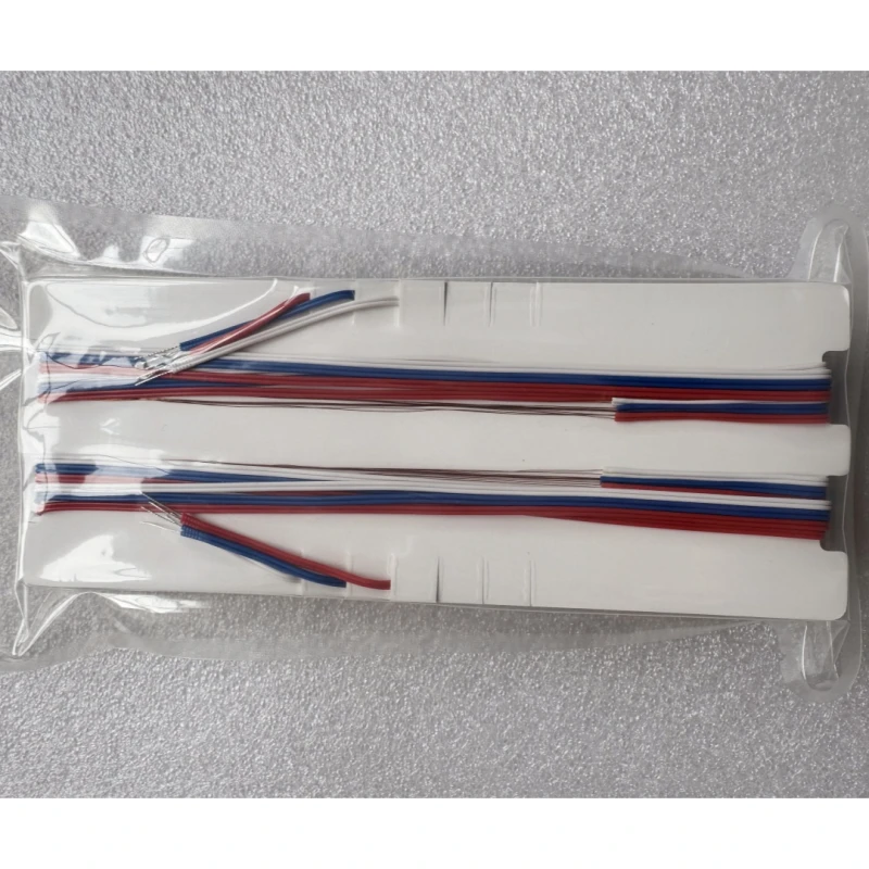
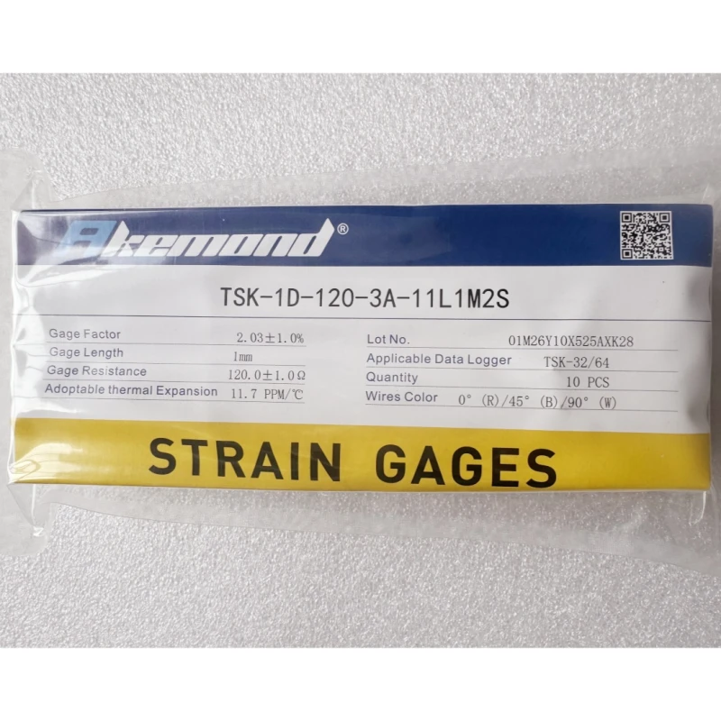
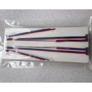
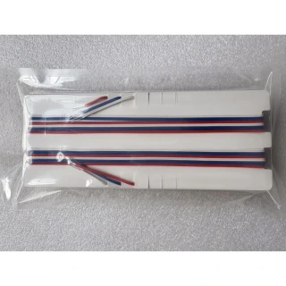
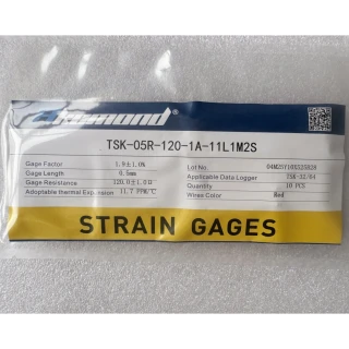
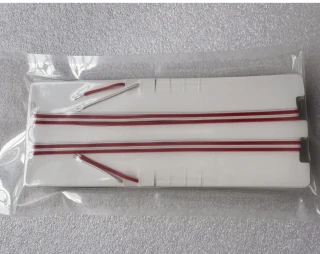
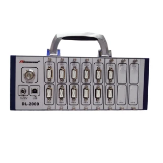
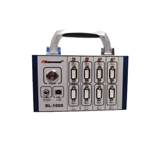
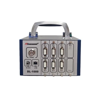
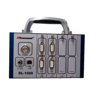
TSK-1D-120-3A-11L1M2S Triaxial Strain Gauge TSK-1D-120-3A-11L3M2S
Specifications
| Device Funtion: | Strain Gauge |
|---|---|
| Measurement Range: | -55500 – 55500 uE |
| Accuracy: | -0.3 – 0.3 % |
| Stability: | 6 ppm/degC |
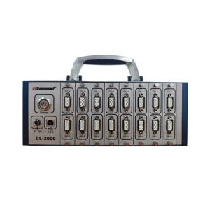
| Sampling Frequency: | 10 KHz (per channel) |
| Operational Temperature Range: | -40 – 70 degC |
| Gauge Type: | Triaxial |
| Impedance: | 120 Ohm |
| Grid Length: | 1.1 x 1.0 mm |
| Base Size: | 2.5 x 2.7 mm |
| Insulated Wire: | 50 cm |
| Extension Wire: | 90 cm |
Got questions about specs? Use the inquiry form to ask.
Features
- Comprehensive PCBA Strain Measurement Solution: Our product offers a complete solution for measuring strain on printed circuit board assemblies (PCBA), ensuring reliability and performance.
- Industry-Standard Compliance: Adheres to IPC/JEDEC-9704A guidelines, the industry benchmark for PCBA strain gage testing, ensuring your processes meet global standards.
- Wide Application Range: Suitable for various stages of PCBA processing, including SMT assembly, panel cutting, manual operations, rework, repair processes, connector installation, and PCB testing.
- Prevention of Common Failures: Helps identify and prevent common mechanical stress-induced failures such as cracked solder balls, circuit damage, warped pads, and substrate cracks.
- Cost-Effective Problem Solving: Early detection of strain issues can save significant costs, following the 1-10-100 rule: $1 during design, $10 during manufacturing, and $100 during production.
- Enhanced Product Reliability: By monitoring and controlling mechanical stresses, manufacturers can reduce defective products, ensuring higher reliability for end customers.
- Adaptation to Modern Materials: Addresses challenges posed by lead-free PCB laminate materials and increased interconnect density, which can lead to warpage and damage.
- Proactive Quality Assurance: Provides systematic steps for performing PCBA strain testing, helping identify defective assembly and test processes before they impact product quality.
Applications
- Typical Processing Needs Strain Measurement
- SMT Assembly
- Panel Cutting
- Manual Operation
- All Rework and Repair Process
- Connector Installation
- PCB Testing
- ICT, FCT, or Equivalent Functional Test
- Mechanical Assembly:
- Heat Sink Assembly
- PCI or Daughterboard Installation
- DIMM (Dual In-line Memory Module) Installation
- Printed Circuit Assembly Strain Gage Test Guideline
- Issued by IPC and JEDEC in 2005
- Revised Version A in 2012
- Identify Defective Assembly and Test Processing
- Provide Systematic Steps to Perform PCBA Strain Testing
- Measurement Standards
- Intel for Strain
- Measurement Purpose
- Solder joints are sensitive to strain, leading to fracture mechanisms due to PCB stress warpage deformation.
- With lead-free new PCB laminate materials and increased interconnect density, damage from warpage has increased.
- Incomplete cracking may not cause immediate PCBA failure and cannot always be detected by functional tests.
- Clients can reduce defective products by effectively monitoring and controlling mechanical stresses during testing and assembly.
Frequently Asked Questions
What is the purpose of PCBA strain measurement?
What are some common failure modes due to mechanical stress in PCBAs?
What is the IPC/JEDEC-9704A guideline?
Why is strain gage testing important during the design phase of PCBA?
What industries promote the use of PCBA strain measurement standards?
How does strain affect solder joints in PCBAs?
What is the cost impact of discovering PCBA problems at different stages?
Got more questions? Use the RFQ form to ask the supplier directly.
Similar Products

Need pricing for this product? Send a quick inquiry
Your inquiry has been received.
Create an account by adding a password
Why create an account?
- Auto-complete inquiry forms
- View and manage all your past messages
- Save products to your favorites
- Close your account anytime — no hassle