


Description
Supplier of Stress Testing Instruments
In the intricate world of electronics manufacturing, ensuring the reliability and durability of printed circuit board assemblies (PCBA) is paramount. As a leading supplier of stress testing instruments, we specialize in providing cutting-edge solutions for PCBA strain measurement. Our expertise in this niche field is backed by years of experience and a commitment to advancing industry standards.
PCBA Strain Measurement Background
Printed circuit board assemblies undergo various stages of manufacturing and testing, including Surface Mount Technology (SMT) assembly, panel cutting, and manual operations. During these processes, PCBAs are subjected to mechanical stresses that can lead to failures such as cracked solder balls, circuit damage, and substrate cracks. These failures not only incur material costs but also impact investments in research and development, production, and troubleshooting efforts.
Industry Standards and Evolution
With the active promotion by global technology leaders like Intel, IBM, HP, and Apple, strain measurement has become a critical standard in the electronics industry. The IPC/JEDEC-9704A guideline, initially issued in 2005 and revised in 2012, serves as a benchmark for identifying defective assemblies and ensuring systematic PCBA strain testing. This standardization has been instrumental in setting industry benchmarks and improving product reliability.
The Importance of Early Detection
Addressing strain-related issues early in the design phase can significantly reduce costs. The principle of "1-10-100" illustrates that a problem costing $1 to fix during design can escalate to $10 during manufacturing and $100 during production. Therefore, early detection and measurement of strain are crucial to minimizing costs and enhancing product quality.
Purpose of Strain Gage Testing
Strain gage testing is essential for understanding the mechanical stresses that affect solder joints and PCB integrity. As the use of lead-free materials and higher interconnect densities become more prevalent, the risk of damage from warpage increases. Strain measurement helps manufacturers monitor and control these stresses, reducing the likelihood of defective products reaching end customers. By implementing effective strain measurement techniques, manufacturers can ensure the longevity and performance of their electronic products.
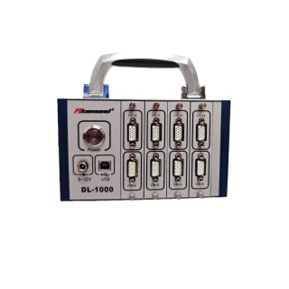
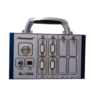
DL-1000-24C-12 PCB Strain Testing System Replacement for Elogger NBM DAQ
Specifications
| Device Funtion: | Data Logger |
|---|---|
| Measurement Range: | -55500 – 55500 uE |
| Accuracy: | -0.3 – 0.3 % |
| Stability: | 6 ppm/degC |
| Sampling Frequency: | 10 KHz (per channel) |
| Operational Temperature Range: | -40 – 70 degC |
| Current Channel: | 24 |
| Max Channel: | 32 |
| Impedance: | 120 Ohm |
Got questions about specs? Use the inquiry form to ask.
 Download Data Sheet

Features
- Comprehensive PCBA Strain Measurement Solutions: Our instruments provide a complete solution for measuring strain on printed circuit board assemblies (PCBA), ensuring reliability and performance.
- Industry Standards Compliance: Adheres to IPC/JEDEC-9704A guidelines, the industry benchmark for PCBA strain gage testing, ensuring your processes meet global standards.
- Wide Range of Applications: Suitable for various stages of PCBA processing, including SMT assembly, panel cutting, manual operations, rework, repair processes, connector installation, and PCB testing.
- Cost-Effective Problem Solving: Address potential issues early in the design phase to save costs, following the 1-10-100 rule, where early detection significantly reduces expenses.
- Enhanced Reliability Testing: Identifies defective assembly and test processes, providing systematic steps for effective PCBA strain testing.
- Prevention of Common Failures: Helps prevent common mechanical stress-induced failures such as cracked solder balls, circuit damage, warped pads, and substrate cracks.
- Support for Lead-Free Materials: Accommodates new PCB laminate materials and increased interconnect density, addressing challenges posed by warpage and deformation.
- Improved Product Quality: Enables manufacturers to monitor and control mechanical stresses, reducing defective products and enhancing customer satisfaction.
- Global Manufacturer Endorsement: Actively promoted by leading global manufacturers like Intel, IBM, HP, and Apple, reinforcing its credibility and effectiveness.
Applications
- Typical Processing Needs Strain Measurement:
- SMT Assembly
- Panel Cutting
- Manual Operation
- All Rework and Repair Process
- Connector Installation
- PCB Testing
- ICT, FCT, or Equivalent Functional Test
- Mechanical Assembly:
- Heat Sink Assembly
- PCI or Daughterboard Installation
- DIMM (Dual In-line Memory Module) Installation
- Common Modes of Failure Due to Mechanical Stress:
- Cracked Solder Balls
- Circuit Damage
- Warped Pads
- Cracked Substrates
- Capacitor Y-Cracks and 45° Cracks
- PCBA Strain Gage Test Guideline:
- Issued by IPC and JEDEC in 2005
- Revised Version A in 2012
- Identify Defective Assembly and Test Processing
- Provide Systematic Steps to Perform PCBA Strain Testing
- Measurement Purpose:
- Solder joints are sensitive to strain, leading to fracture mechanisms.
- Damage caused by warpage increases with lead-free PCB laminate materials and higher interconnect density.
- Incomplete cracking may not cause immediate PCBA failure, undetectable by functional tests.
- Monitoring and controlling mechanical stresses can reduce defective products for end customers.
Frequently Asked Questions
What is the purpose of PCBA strain measurement?
What are some common failure modes due to mechanical stress in PCBAs?
Why is strain gage testing important during the design phase of PCBA?
What are the typical applications that require strain measurement?
What standards govern PCBA strain gage testing?
How does the cost of addressing PCBA issues change over time?
What role do global manufacturers play in PCBA strain measurement standards?
Got more questions? Use the inquiry form to ask the supplier directly.
Similar Products
Your inquiry has been received.
Create an account by adding a password
Why create an account?
- Auto-complete inquiry forms
- View and manage all your past messages
- Save products to your favorites
- Close your account anytime — no hassle