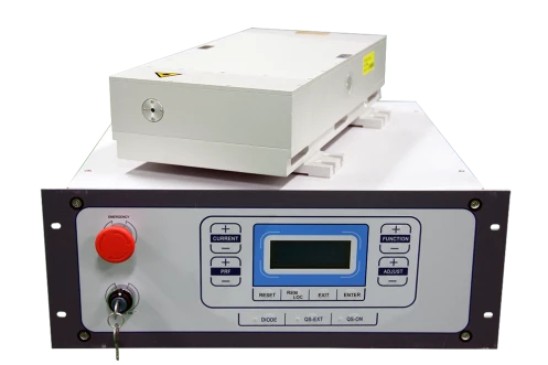
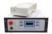
Description
Suzhou Delphi Laser Co., Ltd. (苏州德龙激光有限公司) is a renowned leader in laser technology, located at NO. 77 Suhong Middle Rd, SIP, Suzhou, Jiangsu, China. With a commitment to innovation and quality, the company has developed the MP101 UV Nanosecond Laser, a cutting-edge solution designed to meet the demands of various high-precision applications. This laser stands out with its advanced technology and robust design, making it a reliable choice for industries requiring precision and efficiency.
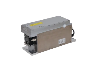
The MP101 UV Nanosecond Laser is engineered with a dual laser diode pumped crystal architecture, delivering high power output at the 355 nm wavelength. This sophisticated design is complemented by an advanced resonant cavity and laser control technology, which ensure superior beam quality and narrow pulse widths even during high power operations. The laser's stability and efficiency are further enhanced by special thermal compensation and harmonic generation technologies, setting a new standard in frequency conversion.
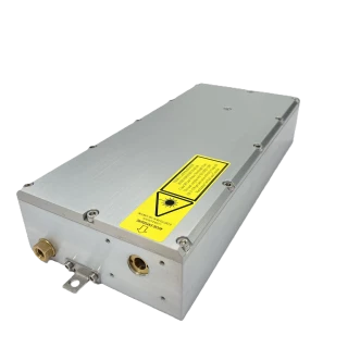
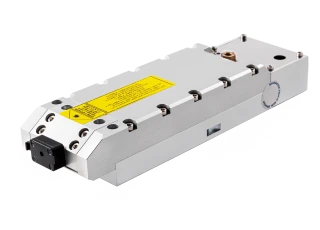
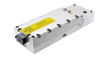
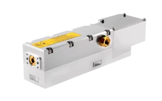
Compactness and durability are key attributes of the MP101, as it features a small size and compact structure that facilitate easy integration into various systems. The laser is assembled in a class 1000 cleanroom, ensuring the highest standards of cleanliness and quality. Additionally, it offers flexibility with its RS232 interface, external GATE, and PWM control, allowing for seamless integration into existing setups. The field-replaceable laser diode module further enhances its usability, ensuring minimal downtime and maintenance.
Operating under a wide range of environmental conditions, the MP101 is equipped with water-cooling to maintain optimal performance. It is designed to function efficiently within ambient temperatures of 15 to 30 degrees Celsius and can be stored in temperatures ranging from -10 to 50 degrees Celsius. The laser's robust design and high long-term stability make it an ideal choice for industries seeking reliable and precise laser solutions.
5-7W UV DPSS Laser Source
Specifications
| Avg. Power: | 7 W |
|---|---|
| Wavelength: | 355 nm |
| Repetition Rate: | 20 – 100 kHz |
| Spatial Mode (M^2): | 1.3 |
| Pulse Duration: | 25 ns |
| Pulse-to-Pulse Stability (RMS): | 3 % |
| Cooling: | Water-to-Water |
| Model Number: | MP101 |
Got questions about specs? Use the inquiry form to ask.
Features
- High Power Output: The MP101 UV Nanosecond Laser features a dual laser diode pumped crystal architecture, delivering high power output at a 355 nm wavelength.
- Advanced Beam Quality: Designed with advanced resonant cavity and laser control technology, ensuring excellent beam quality and narrow pulse widths during high power operation.
- Stable Frequency Conversion: Special thermal compensation and harmonic generation technologies provide stable and efficient frequency conversion.
- Versatile Pulse Repetition Rate: Offers a pulse repetition rate of 20 – 100 kHz, adjustable up to 150 kHz for various applications.
- Precision and Stability: Achieves a spatial mode of TEM00 with M2 < 1.3, ensuring high long-term stability and precision.
- Compact Design: Features a small size and compact structure, making it suitable for various installation environments.
- Easy Integration: Equipped with RS232, external GATE, and PWM control for seamless integration into existing systems.
- Field-Replaceable Components: The laser diode module is field-replaceable, ensuring easy maintenance and reduced downtime.
- Cleanroom Assembled: Assembled in a class 1000 cleanroom to maintain high quality and reliability.
- Wide Range of Applications: Ideal for film etching, laser marking, material micromachining, wafer cutting, micro-drilling, laser rapid prototyping, and scientific research.
- Efficient Cooling: Utilizes water-cooling to maintain optimal operating temperature.
- Wide Operating Conditions: Operates efficiently within an ambient temperature range of 15 – 30℃ and relative humidity of 10%-80% (non-condensing).
- Quick Start-Up: Warm-up time of less than 10 minutes for rapid deployment.
- Flexible Power Requirements: Operates on a wide voltage range of 90 – 260 V, accommodating various power supply conditions.
Applications
- Film Etching: Enables precise patterning of thin film materials.
- Laser Marking: Provides high-contrast, durable markings on various substrates.
- Material Micromachining: Supports fine microfabrication with minimal thermal damage.
- Wafer Cutting: Ideal for semiconductor wafer dicing and scribing.
- Micro-Drilling: Performs high-precision drilling of micro-holes in diverse materials.
- Laser Rapid Prototyping: Enhances additive manufacturing processes with UV precision.
- Scientific Research: Suitable for advanced photonics and materials research.
Frequently Asked Questions
What are the applications of the MP101 UV laser?
What is the average power output of the MP101 UV laser?
What is the pulse repetition rate of the MP101 UV laser?
What is the wavelength of the MP101 UV laser?
What is the cooling system used for the MP101 UV laser?
Got more questions? Use the RFQ form to ask the supplier directly.
Similar Products


Need pricing for this product? Send a quick inquiry
Your inquiry has been received.
Create an account by adding a password
Why create an account?
- Auto-complete inquiry forms
- View and manage all your past messages
- Save products to your favorites
- Close your account anytime — no hassle