

Description
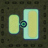
The CCSiCUVAPD1p1 silicon carbide (SiC) ultraviolet avalanche photodiode delivers highly sensitive UV detection in the 200–375 nm range while maintaining inherent blindness to visible light. Engineered on high-quality SiC epitaxial layers, this device is optimized for applications where deep‑UV performance, extremely low dark current, and long‑term stability under harsh operating conditions are critical. With a typical peak linear responsivity of 0.07 A/W and a corresponding peak quantum efficiency of 32% at 270 nm (M = 1), it provides a robust platform for both linear and Geiger-mode UV photon counting in demanding scientific, industrial, and defense‑related environments.
CoolCAD Electronics’ silicon carbide (SiC) avalanche photodiodes (APDs) provide a high-sensitivity alternative to conventional silicon photodiodes for demanding photodetection applications, particularly at elevated temperatures. While traditional silicon photodiodes and silicon APDs experience rapidly increasing dark current and noise as temperature rises, SiC’s wide bandgap (~3.2 eV) and high critical electric field enable exceptionally low dark current and stable avalanche operation under extreme thermal conditions. CoolCAD’s SiC APDs are designed to maintain high gain and low noise at temperatures exceeding 300°C, extending reliable photon detection well beyond the practical temperature range of conventional silicon-based detectors.
In addition to their high-temperature capability, these APDs provide intrinsic avalanche multiplication for detecting extremely weak optical signals, including single-photon-level events, without requiring the external amplification associated with conventional photodiodes. Strong avalanche gain is achieved at approximately 180–200 V reverse bias, with future designs targeting operation near 100 V. The resulting solid-state detectors combine high sensitivity, low noise, UV-selective response, and resistance to mechanical shock and vibration, offering a compact and rugged alternative to both conventional silicon detectors and mechanically fragile photomultiplier tubes in applications such as downhole sensing, geothermal instrumentation, industrial flame detection, aerospace sensing, and UV spectroscopy.
Unlike conventional silicon UV photodiodes that often require optical filters and cooling to suppress visible background and thermal noise, the CCSiCUVAPD1p1 offers intrinsic visible‑blind operation and ultra‑low dark current (typically < 5 pA/mm² at VR < 3 V, 25°C). This combination reduces system complexity and volume by eliminating the need for additional blocking filters and active cooling hardware, which is particularly advantageous in compact, battery‑powered, or remote sensing platforms. The device’s active area of 0.019 mm² and capacitance of 15 pF at low bias support fast response times and low noise, making it well suited for high‑speed UV monitoring and time‑resolved measurements.
The spectral response of the CCSiCUVAPD1p1 is tightly centered around the germicidal and solar‑blind UV region. Its 90% maximum QE window lies approximately between 265 nm and 275 nm, while the full‑width‑at‑half‑maximum quantum efficiency spans roughly 240 nm to 315 nm. This spectral profile aligns closely with many industrial and scientific standards for UV‑C and UV‑B detection, allowing precise monitoring of sources such as excimer lamps, UV LEDs, and plasma discharges. A visible‑blindness ratio greater than 5000 (peak UV responsivity to responsivity at 400 nm) helps ensure that measured signals correspond predominantly to the target UV band, even in environments with strong ambient visible illumination.
In avalanche mode, the CCSiCUVAPD1p1 is designed to reach very high gain while maintaining stable operation. The avalanche breakdown voltage is carefully binned into narrow ranges, with typical subsets between approximately 195 V and 203 V, enabling better control in array configurations and high‑precision bias circuits. Under 270 nm illumination at the breakdown voltage, achievable gain exceeds 105, supporting single‑photon level detection and Geiger‑mode operation for photon counting. This makes the device a strong candidate for UV lidar receivers, fluorescence lifetime measurements, and high‑sensitivity lab instrumentation that previously depended on bulkier photomultiplier tubes or less robust silicon APDs.
The SiC construction of the CCSiCUVAPD1p1 delivers excellent thermal and radiation robustness. It is engineered to operate over a very wide temperature range, with no degradation reported up to temperatures on the order of 400°C in typical SiC device use cases. Combined with demonstrated resilience to prolonged UV exposure and ionizing radiation, this makes the photodiode particularly attractive for aerospace and satellite payloads, high‑temperature industrial applications.
CoolCAD CCSiCUVAPD1p1 SiC Ultraviolet Avalanche Photodiode 200-375nm
Specifications
| APD Type: | Silicon Carbide (SiC) |
|---|---|
| Operational Wavelength (Typical): | 270 nm |
| Operational Wavelength Range: | 200 – 375 nm |
| Peak Linear Responsivity (Rmax): | 0.07 A/W |
| Peak Linear Quantum Efficiency: | 0.32 |
| Active Area: | 0.019 mm^2 |
| Part Number: | CCSiCUVAPD1p1 |
| Peak Linear Responsivity: | 0.07 A/W @ VR < 3 V, λ = 270 nm, TA = 25°C, M = 1 |
| Peak Linear Quantum Efficiency: | 0.32 @ VR < 3 V, λ = 270 nm, TA = 25°C, M = 1 |
| Spectral Range (90% Max QE): | 265–275 nm @ VR < 3 V, TA = 25°C, M = 1 |
| Spectral Range (FWHM QE): | 240–315 nm @ VR < 3 V, TA = 25°C, M = 1 |
| Dark Current: | < 5 pA/mm² @ VR < 3 V, TA = 25°C, M = 1 |
| Visible Blindness Ratio: | > 5000 (peak responsivity / responsivity @ 400 nm, VR = 2 V, M = 1) |
| Active Area: | 0.019 mm² |
| Avalanche Breakdown Voltage (CCSiCUVAPD1p1A): | 195–197 V @ ID = 1 µA, TA = 25°C |
| Avalanche Breakdown Voltage (CCSiCUVAPD1p1B): | 198–200 V @ ID = 1 µA, TA = 25°C |
| Avalanche Breakdown Voltage (CCSiCUVAPD1p1C): | 201–203 V @ ID = 1 µA, TA = 25°C |
| Gain: | > 1E5 @ VR = Vbd,av, λ = 270 nm |
| Capacitance: | 15 pF @ VR < 3 V, TA = 25°C, M = 1 |
| Maximum Operating Temperature (no Degradation): | up to 400°C |
| Package: | Bare die (no package) |
Got questions about specs? Use the inquiry form to ask.
 Download Data Sheet

Features
- Deep UV Sensitivity (200–375 nm) – Optimized SiC avalanche photodiode for ultraviolet detection in the 200–375 nm range, ideal for UV-C and UV-B applications including sterilization monitoring, flame and corona detection, and UV spectroscopy.
- High Quantum Efficiency at 270 nm – Peak linear quantum efficiency of ~32% and responsivity of 0.07 A/W at 270 nm (VR < 3 V, M = 1), delivering strong signal levels for narrowband UV sources such as excimer lamps and UV LEDs.
- Narrowband UV Response Window – Spectral range (90% of max QE) of 265–275 nm and FWHM QE range of 240–315 nm, enabling selective UV-C/B detection with minimal out-of-band response and improved signal-to-noise in UV-specific systems.
- True Solar-Blind / Visible-Blind Operation – Visible blindness ratio > 5000:1 (peak responsivity vs. 400 nm), eliminating the need for external optical filters and providing robust rejection of ambient and solar visible light in outdoor and high-background environments.
- Ultra-Low Dark Current – Dark current < 5 pA/mm² at VR < 3 V and 25 °C, dramatically reducing noise floor and enabling highly sensitive detection of weak UV signals and single-photon events.
- High Internal Gain in Avalanche Mode – Avalanche gain > 1 × 10⁵ at breakdown bias, allowing operation in Geiger mode for single-photon counting and time-resolved UV photon detection in scientific and industrial instruments.
- Engineered Breakdown Voltage Binning – Available breakdown voltage bins (e.g., 195–203 V ranges) simplify biasing design, ensure predictable gain characteristics, and improve uniformity in multi-pixel and array-based detection systems.
- Compact Active Area for High Spatial Resolution – Active area of approximately 0.019 mm² supports high-resolution spot detection, tight focusing, and dense arrays for imaging, position sensing, and fiber-coupled UV detection.
- Low Capacitance for Fast Response – Typical capacitance of 15 pF (VR < 3 V, M = 1) enables high-speed detection, sharp pulse response, and compatibility with fast readout electronics in time-correlated and counting applications.
- Wide Temperature Operation up to 400 °C – SiC-based design maintains performance across an exceptionally wide temperature range (up to ~400 °C) with no degradation, ideal for harsh and high-temperature environments such as combustion chambers and industrial process lines.
- Excellent UV & Radiation Hardness – Intrinsic robustness under long-term UV exposure and ionizing radiation provides stable responsivity and long lifetime in space, nuclear, high-intensity UV curing, and sterilization systems.
- No Cooling or Filters Required – Combination of low dark current, visible blindness, and wide thermal tolerance minimize system complexity by removing the need for thermoelectric cooling, shutters, or external UV bandpass filters, reducing total cost and footprint.
- SiC Material Advantages Over Silicon – Compared with conventional silicon photodiodes and APDs, SiC devices deliver lower leakage current, much higher UV-to-visible selectivity, better thermal stability, and superior durability in demanding operating conditions.
- Geiger and Linear Mode Operation – Supports both linear mode for analog UV intensity measurements and Geiger mode for digital single-photon counting, adaptable to a wide range of scientific, industrial, and safety monitoring tasks.
- Ideal for Critical UV Applications – Engineered for use in water and air purification monitoring, pathogen detection, flame and spark detection, semiconductor process monitoring, UV curing control, leak detection, and defect inspection.
- Bare Die Format for Flexible Integration – Supplied as a bare die, enabling custom packaging, optical coupling (lenses, fibers, windows), and direct integration into compact modules, arrays, and ASIC-based detector systems.
- Customizable to Application Requirements – Fabricated on high-quality SiC epitaxial layers using proprietary processes, allowing customization of active area, breakdown voltage, packaging, and array configurations to meet specific OEM and research needs.
- Stable, Repeatable Performance – Carefully controlled breakdown characteristics, low noise, and robust UV response support consistent, repeatable measurements essential for calibrated instruments and regulatory-compliant monitoring systems.
- Solar UV Monitoring and Environmental Sensing – High-accuracy monitoring of solar ultraviolet radiation (200–375 nm) for climate research, ozone layer studies, atmospheric chemistry, and long-term outdoor UV index stations without the need for cooling or optical visible filters.
- Flame Detection and Fire Safety Systems – Early flame detection in industrial burners, gas turbines, boilers, and fire alarm systems using UVC/UVB emissions for fast response and high immunity to sunlight and artificial visible lighting.
- Gas and Plasma Discharge Monitoring – Detection of UV emissions from corona discharges, arc faults, electric switchgear, plasma reactors, and high-voltage equipment for predictive maintenance and fault localization.
- Water and Air UV Disinfection System Monitoring – Real-time feedback and dose monitoring in UV-C water purification, wastewater treatment, ballast water treatment, and air sterilization units (e.g., 254–280 nm germicidal lamps and UV-C LEDs).
- Pathogen and Bio-Hazard Detection – UV-induced fluorescence and direct UVC detection for identifying biological agents, bacteria, and viruses in medical diagnostics, bio-safety cabinets, and environmental pathogen monitoring systems.
- Semiconductor and Photomask Inspection – Defect inspection, line edge roughness analysis, and particle detection on wafers and photomasks using deep-UV illumination, leveraging visible-blind response and very low dark current.
- Surface and Coating Defect Monitoring – UV reflectometry and fluorescence-based quality control of paints, anti-corrosion coatings, UV-curable resins, adhesives, and protective layers in industrial production lines.
- Single-Photon Counting in the UV – Geiger-mode operation for low-light and single-photon detection in time-correlated single-photon counting (TCSPC), fluorescence lifetime measurements, and quantum optics experiments in the UV.
- Time-Resolved Spectroscopy and Fluorescence Measurements – Detection of fast UV fluorescence and phosphorescence decays in materials research, scintillator characterization, and biochemical assays requiring high gain and fast response.
- Scintillation and High-Energy Physics Detection – Readout of UV-emitting scintillators used in nuclear instrumentation, particle physics, radiation monitoring, and homeland security detectors.
- Spaceborne and Aerospace UV Sensors – Radiation-hardened UV detection for satellite instruments, space telescopes, rocket payloads, and planetary/atmospheric missions where robustness to radiation and extreme temperatures is critical.
- Missile Plume and Rocket Exhaust Detection – UV-based missile launch and plume detection systems with strong solar blindness, suitable for defense early-warning sensors and rocket exhaust diagnostics.
- Industrial UV Process Control – In-line monitoring of UV curing of inks, coatings, and adhesives, ensuring proper dose and uniformity in printing, lithography, and 3D printing applications.
- UV LED and Lamp Characterization – Radiometric measurements and lifetime testing of UV-C and UV-B LEDs, excimer lamps, and mercury lamps, including power monitoring, spectral stability, and aging behavior.
- Laser Diagnostics in the UV – Power, pulse, and beam stability monitoring for UV lasers (e.g., 248 nm, 266 nm, excimer and frequency-quadrupled solid-state lasers), including alignment and feedback control.
- UV Spectrophotometry and Spectroscopy Detectors – Use as a detector in monochromator-based UV spectrometers for chemical analysis, thin-film characterization, and optical component testing in the 200–375 nm range.
- Security and Anti-Counterfeiting – Reading UV-sensitive security inks, markers, and tags on banknotes, IDs, product packaging, and high-value documents where visible-blind detection reduces false positives.
- Industrial UV Imaging Systems (with Optics/Arrays) – Implementation in arrays or scanned setups for UV imaging of surfaces, contamination, micro-cracks, and defects that are invisible in the visible spectrum.
- Combustion and Engine Diagnostics – In-cylinder and exhaust UV emission monitoring for combustion research, engine optimization, and NOx/OH radical studies in automotive, aerospace, and power generation.
- Scientific Instrumentation and Metrology – Integration into precision UV radiometers, dosimeters, and calibration standards for metrology labs and reference instruments across the 240–315 nm FWHM QE range.
Applications
Frequently Asked Questions
What is the CCSiCUVAPD1p1 SiC ultraviolet avalanche photodiode and what wavelengths does it detect?
How does the CCSiCUVAPD1p1 compare to standard silicon UV photodiodes and APDs?
What are the key electrical and optical specifications of the CCSiCUVAPD1p1?
How do I bias and read out the CCSiCUVAPD1p1 in linear mode versus Geiger (single‑photon) mode?
What packaging options, handling requirements, and mounting guidelines apply to the CCSiCUVAPD1p1?
What applications are best suited for the CCSiCUVAPD1p1 SiC UV avalanche photodiode?
Can the CCSiCUVAPD1p1 be customized, and what parameters are typically adjustable?
Got more questions? Use the inquiry form to ask the supplier directly.
Similar Products


Your inquiry has been received.
Create an account by adding a password
Why create an account?
- Auto-complete inquiry forms
- View and manage all your past messages
- Save products to your favorites
- Close your account anytime — no hassle