
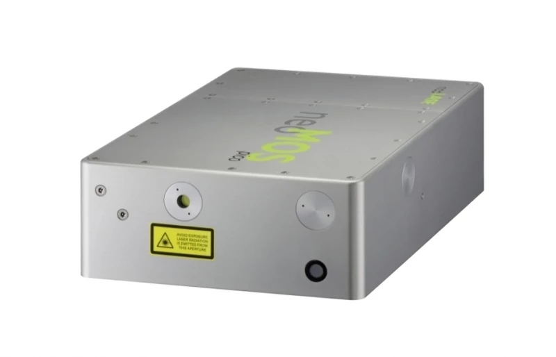
Description
neoLASE neoMOS Industrial Picosecond Laser Overview
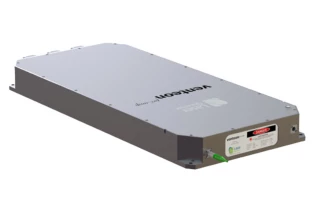
The neoLASE neoMOS Industrial Picosecond Laser is a compact, high-performance ultrafast laser source designed for precision industrial material processing. Built around advanced MOPA picosecond laser technology, the neoMOS series combines the reliability of a laser diode seed source with the performance of a solid-state amplifier, delivering stable picosecond pulses for demanding 24/7 production environments.
With operation at 1064 nm, pulse durations of approximately 70 ps, and output power up to 15 W, the neoMOS laser is well suited for applications requiring clean, controlled energy deposition with minimal thermal impact. Its picosecond pulse regime enables high-quality micromachining, precision laser marking, fine ablation, structuring, drilling, trimming, and cutting across a wide range of materials, including metals, ceramics, semiconductors, transparent glass, and technical plastics.
Compared with conventional nanosecond laser systems, this industrial picosecond laser supports colder processing with reduced heat-affected zones, cleaner edges, and improved surface quality. This makes it particularly valuable for manufacturers working with sensitive substrates, miniaturized components, and high-value parts where repeatability, accuracy, and process stability are critical. The system’s high beam quality, with near-TEM operation and low M² performance, supports precise focusing for micro-scale processing tasks.
The neoMOS series is engineered for flexible process development and easy integration into industrial laser workstations, OEM machines, and automated production lines. Its ability to support flexible repetition rates, from single-shot operation up to high-frequency operation, allows users to optimize throughput, pulse energy, and process quality for different materials and geometries. This makes the laser adaptable to both research-driven process development and continuous manufacturing environments.
As a compact industrial picosecond laser source, the neoLASE neoMOS is positioned for applications where reliability, long-term stability, and low maintenance are essential. Its ultra-compact laser head simplifies system design, while its robust architecture supports high uptime in production settings. For precision micromachining, ultrafast laser processing, and advanced materials manufacturing, the neoMOS provides a strong balance of power, pulse control, beam quality, and industrial durability.
neoMOS-70ps: Picosecond Laser
Specifications
| Center Wavelength: | 1064 nm |
|---|---|
| Repetition Rate: | 0.001 – 80000 kHz |
| Pulse Energy: | 0.25 mJ |
| Energy Stability (RMS): | 1 % |
| Pulse Duration: | 70000 fs |
| Polarization: | Unspecified |
| Spatial Mode (M^2): | <1.3 |
| Amplification Scheme: | Not Specified |
| Average Power: | 15 W |
| Polarization Ratio: | >100:1 |
| Warm-up Time: | <30 min. |
| Laser Controller: | 19'' Rackmount 6 U height |
| Cooling: | Water cooled |
| Options: | SHG |
Got questions about specs? Use the inquiry form to ask.
 Download Data Sheet

Features
- Output power: 15 W @ 1064 nm
- Pulse duration: 70 ps
- Pulse energy: Up to 250 µJ
- Repetition rates: Single shot to 80 MHz, Flex Pulse
- Beam quality: TEM0,0 / M²<1.3
- Flexible repetition rate and pulse energy
- Ultra-compact laser head design
- Proven long term stability and industrial reliability
Applications
The neoLASE neoMOS industrial picosecond laser is designed for high-precision, 24/7 material processing where ultrashort pulses, high peak power, excellent beam quality, and flexible repetition rates are required. With 70 ps pulse duration, up to 250 µJ pulse energy, 15 W output power at 1064 nm, and flex pulse operation from single shot to high repetition rates, it is well suited for demanding micromachining, marking, structuring, and cutting applications across industrial and research environments.
- Precision micromachining: High-quality laser micromachining of metals, ceramics, glass, polymers, composites, and coated materials with minimal heat-affected zone and excellent edge quality.
- Laser marking and engraving: Permanent, high-contrast marking of metals, plastics, ceramics, glass, and technical components for traceability, branding, serialization, QR codes, barcodes, and industrial identification.
- Fine cutting and micro-cutting: Precise cutting of thin metals, foils, ceramics, brittle materials, polymers, and multilayer substrates where low thermal damage and clean kerf geometry are critical.
- Glass processing: Picosecond laser processing of transparent and brittle glass materials, including glass cutting, scribing, drilling, edge shaping, internal modification, and micro-structuring for display, optics, and sensor manufacturing.
- Transparent material processing: Efficient processing of transparent glasses and plastics using high peak power ultrafast pulses for applications that require localized energy deposition and controlled material modification.
- Plastic and polymer processing: Fine laser marking, ablation, texturing, cutting, and drilling of plastics and polymers with reduced melting, charring, or deformation compared to longer-pulse laser sources.
- Thin-film ablation: Selective removal of thin films, functional coatings, conductive layers, oxides, and dielectric materials used in electronics, photovoltaics, displays, and sensor production.
- Surface structuring and texturing: Creation of micro- and nano-scale surface features for improved adhesion, wettability control, friction reduction, light management, anti-counterfeiting, decorative effects, and functional surface engineering.
- Micro-drilling: High-precision drilling of micro-holes in metals, ceramics, glass, polymers, and hard materials for filters, nozzles, medical devices, microfluidics, electronics, and precision engineering components.
- Electronics manufacturing: Laser processing for printed circuit boards, flexible electronics, semiconductor packaging, connector components, sensor substrates, thin-film circuits, and microelectronic assemblies.
- Semiconductor and wafer processing: Precision laser ablation, trimming, marking, scribing, and micro-structuring of semiconductor wafers, silicon, compound semiconductors, and related electronic materials.
- Ceramic machining: Fine cutting, drilling, scribing, and structuring of alumina, zirconia, aluminum nitride, silicon nitride, and other technical ceramics used in electronics, medical, aerospace, and industrial applications.
- Metal micromachining: Picosecond laser ablation, engraving, drilling, trimming, and structuring of stainless steel, copper, aluminum, titanium, precious metals, and specialty alloys with high precision and low thermal distortion.
- Medical device manufacturing: Precision processing of medical implants, surgical tools, stents, micro-components, catheters, diagnostic devices, and biocompatible materials requiring clean, repeatable, and highly controlled laser interaction.
- Automotive component processing: Laser marking, micro-drilling, surface texturing, sensor component processing, battery material processing, and precision machining of metal and polymer parts for automotive and e-mobility manufacturing.
- Battery and energy storage applications: Precision processing of battery foils, electrode materials, current collectors, separator films, tabs, and functional coatings for lithium-ion battery development and production.
- Photovoltaic manufacturing: Laser scribing, edge isolation, thin-film removal, patterning, and selective ablation for solar cells, photovoltaic modules, and thin-film solar technologies.
- Display and touch-panel manufacturing: Processing of glass panels, transparent conductive oxides, thin films, polymers, and display substrates used in LCD, OLED, microLED, and touch-screen production.
- Optics and photonics fabrication: Micro-structuring, marking, trimming, and precision modific
Frequently Asked Questions
What are the potential applications for the neoMOS 70ps Picosecond Laser?
Can you list the key features of the neoMOS 70ps Picosecond Laser?
What advantages does the neoMOS 70ps Picosecond Laser offer?
What does the flex pulse control in the neoMOS 70ps Picosecond Laser do?
What are the system specifications for this laser?
What is the warm-up time for the neoMOS 70ps Picosecond Laser?
What cooling requirements does the neoMOS 70ps Picosecond Laser have?
Got more questions? Use the inquiry form to ask the supplier directly.
Similar Products
Your inquiry has been received.
Create an account by adding a password
Why create an account?
- Auto-complete inquiry forms
- View and manage all your past messages
- Save products to your favorites
- Close your account anytime — no hassle