
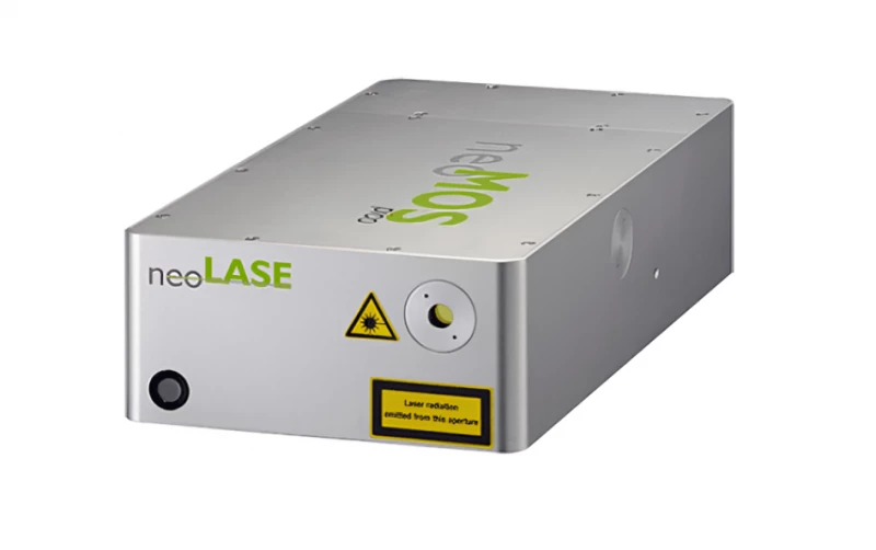
Description
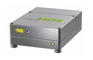
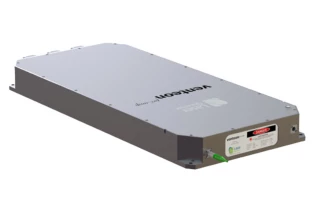
The neoMOS Femtosecond Laser series offers a compact laser head design with highly flexible and scalable features. With an output power of over 50 W, pulse duration less than 700 fs, and pulse energy exceeding 500 µJ, this laser system provides reliability and low maintenance. It combines femtosecond laser oscillators with a power and energy scaling solid-state amplifier, enabling bandwidth-limited, high-energy pulses on a small footprint.
neoMOS-700fs: Femtosecond Laser
Specifications
| Center Wavelength: | 1064 nm |
|---|---|
| Repetition Rate: | 0.001 – 1000 kHz |
| Pulse Energy: | 0.5 mJ |
| Energy Stability (RMS): | 1 % |
| Pulse Duration: | 700 fs |
| Polarization: | Unspecified |
| Spatial Mode (M^2): | <1.3 |
| Amplification Scheme: | Not Specified |
| Output Power: | > 50 W |
| Polarization Ratio: | >100:1 |
| Warm-up Time: | <30 min. |
| Laser Controller: | 19'' Rackmount 4 U height |
| Cooling: | Water cooled |
| Options: | SHG |
Got questions about specs? Use the inquiry form to ask.
 Download Data Sheet

Features
Key Features of the neoLASE neoMOS Femtosecond Laser
- High-power femtosecond laser performance: Delivers >50 W output power for demanding ultrafast laser processing, scientific research, and industrial micromachining applications.
- Ultrashort pulse duration: Generates pulses of <700 fs, enabling precise “cold” laser material processing with minimal heat-affected zone.
- High pulse energy: Provides >500 µJ pulse energy for efficient nonlinear optics, high-throughput microprocessing, and advanced photonics applications.
- Flexible repetition rate operation: Supports repetition rates from single shot to MHz, allowing optimization for both high-energy and high-throughput processing requirements.
- Excellent beam quality: Features TEM00 beam profile with M² < 1.3 for accurate focusing, stable beam delivery, and consistent process results.
- MOPA-based ultrafast laser architecture: Combines a reliable femtosecond oscillator with a power- and energy-scaling solid-state amplifier for stable, scalable output.
- Bandwidth-limited high-energy pulses: Designed to deliver high-quality femtosecond pulses suitable for precision laser processing and nonlinear frequency conversion.
- Compact laser head design: Small-footprint system architecture simplifies integration into laboratory setups, OEM platforms, and industrial workstations.
- Highly scalable and flexible design: Engineered for application-specific configurations, making it suitable for customized ultrafast laser solutions.
- Low-maintenance operation: Solid-state laser technology supports long-term reliability and reduced maintenance requirements compared with more complex ultrafast laser systems.
- Optimized for cold laser processing: Sub-picosecond pulse duration minimizes thermal damage, burr formation, melting, and microcracking in sensitive materials.
- Ideal for precision micromachining: Suitable for micro-drilling, micro-cutting, surface structuring, thin-film ablation, wafer processing, and high-precision material removal.
- Supports nonlinear optics applications: High peak power and excellent beam quality make the system suitable for higher harmonic generation, ultrafast spectroscopy, and advanced photonics research.
- Suitable for OPCPA pumping: High pulse energy and stable femtosecond output support use in optical parametric chirped-pulse amplification systems.
- Versatile material compatibility: Enables precise processing of metals, semiconductors, ceramics, glass, polymers, composites, and other heat-sensitive materials.
- Industrial and scientific use: Well suited for research laboratories, laser material processing centers, semiconductor manufacturing, medical device production, and OEM ultrafast laser integration.
Applications
- Cold laser micromachining: Precision femtosecond laser processing with minimal heat-affected zone for high-quality cutting, drilling, structuring, and ablation of sensitive materials.
- High-precision micro drilling: Production of micro holes, nozzles, filters, injector components, medical device features, and fine apertures in metals, ceramics, glass, polymers, and composites.
- Ultrafast laser cutting: Clean cutting of thin metals, foils, glass, sapphire, ceramics, silicon, polymers, and multilayer materials with reduced burrs, cracks, melting, and recast.
- Glass and transparent material processing: Femtosecond laser cutting, internal modification, selective ablation, scribing, dicing, and 3D structuring of glass, fused silica, quartz, and optical materials.
- Sapphire and ceramic machining: Crack-free micro processing of hard and brittle materials used in optics, electronics, sensors, LEDs, watch components, and high-performance industrial parts.
- Semiconductor wafer processing: Wafer dicing, scribing, edge trimming, micro structuring, defect repair, and thin-film patterning for silicon, compound semiconductors, MEMS, and advanced packaging.
- Microelectronics manufacturing: Precision ablation, via drilling, patterning, trimming, and structuring for PCBs, flexible circuits, interposers, sensors, displays, and miniaturized electronic components.
- Thin-film removal and patterning: Selective laser ablation of conductive, dielectric, metallic, and functional coatings for photovoltaics, displays, touch panels, microelectronics, and sensor devices.
- Photovoltaic and solar cell processing: Laser scribing, edge isolation, thin-film structuring, contact opening, and precision ablation for crystalline silicon and thin-film solar technologies.
- Medical device manufacturing: High-accuracy laser cutting and texturing of stents, catheters, implants, surgical tools, microneedles, biosensors, and diagnostic components with excellent edge quality.
- Surface texturing and functionalization: Creation of micro and nano surface structures to control friction, wettability, adhesion, biocompatibility, light absorption, anti-counterfeiting features, and tribological performance.
- Laser marking and engraving: Permanent high-resolution marking, micro engraving, serial coding, logo marking, and anti-counterfeit structuring on metals, ceramics, glass, polymers, and coated materials.
- Precision metal processing: Ultrafast ablation, drilling, cutting, and surface modification of stainless steel, titanium, aluminum, copper, precious metals, and specialty alloys with limited thermal damage.
- Polymer and composite processing: Clean micro cutting, drilling, surface activation, and patterning of polymers, films, laminates, carbon-fiber composites, and biomedical plastics.
- MEMS and sensor fabrication: Micro structuring, cavity formation, release processes, wafer-level trimming, and precision patterning for MEMS, microfluidics, pressure sensors, accelerometers, and photonic sensors.
- Microfluidics and lab-on-a-chip fabrication: Direct writing, channel formation, drilling, and surface modification in glass, polymers, fused silica, and hybrid substrates for biomedical and analytical devices.
- Optics and photonics manufacturing: Fabrication of micro optics, diffractive optical elements, waveguides, photonic structures, optical gratings, fiber components, and precision optical features.
- 3D laser micro structuring: Direct femtosecond laser writing and localized material modification for complex micro-scale geometries, internal structures, and high-aspect-ratio features.
- Nonlinear optics research: High-peak-power femtosecond pulses for nonlinear frequency conversion, supercontinuum generation, optical parametric processes, and ultrafast light-matter interaction studies.
- OPCPA pumping: High-energy femtosecond laser source for optical parametric chirped-pulse amplification systems used in ultrafast science and high-intensity laser research.
- Higher harmonic generation: Generation of UV, deep-UV, and extreme-ultraviolet radiation through nonlinear harmonic conversion for spectroscopy, microscopy, and advanced research applications.
- Ultrafast spectroscopy: Pump-probe experiments, time-resolved measurements, carrier dynamics studies, and femtosecond-scale investigation of materials, semiconductors, molecules, and nanostructures.
- Terahertz generation and detection: Femtosecond laser exc
Frequently Asked Questions
What applications can benefit from the neoMOS 700fs Femtosecond Laser?
What are the key features of the neoMOS 700fs Femtosecond Laser?
What are the advantages of using the neoMOS 700fs Femtosecond Laser?
What are the system specifications of the neoMOS 700fs Femtosecond Laser?
How long does it take for the neoMOS 700fs Femtosecond Laser to warm up?
Is there a cooling requirement for the neoMOS 700fs Femtosecond Laser?
Are there any safety precautions to consider when using the neoMOS 700fs Femtosecond Laser?
Got more questions? Use the inquiry form to ask the supplier directly.
Similar Products
Your inquiry has been received.
Create an account by adding a password
Why create an account?
- Auto-complete inquiry forms
- View and manage all your past messages
- Save products to your favorites
- Close your account anytime — no hassle