


Description
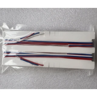
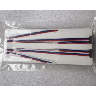
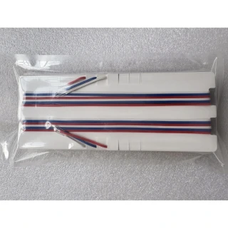
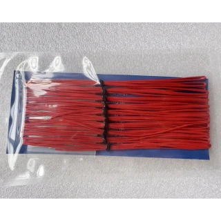
Veshay PCB Strain Gauges Measurement System
PCB Strain testing allows objective analysis of the strain and strain rate levels that a SMT package is subjected to during PWB assembly, test and operation.
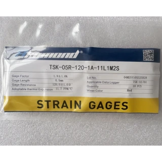
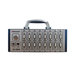
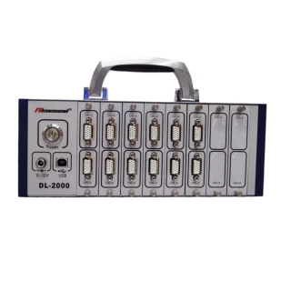
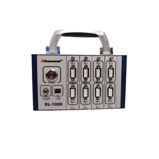
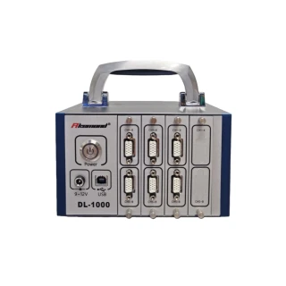
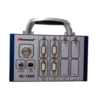
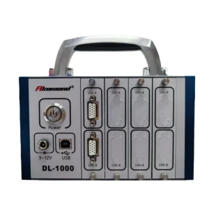
The Veshay PCB Strain Measurement System is special design for printed wiring board strain testing application. The real-time data provided by the Veshay system avoid the risk such failures include solder ball cracking, trace damage, pad lifting and substrate cracking during board manufacturing and test processes.
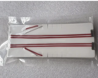
Veshay Akemond PCB Strain Gauges TSK-1D-120-3A-11L50W05MS IPC/JEDEC 9704 PCB Strain Testing Dynamic Strain Meter
Specifications
| Device Funtion: | Strain Gauge |
|---|---|
| Measurement Range: | -55500 – 55500 uE |
| Accuracy: | -0.3 – 0.3 % |
| Stability: | 6 ppm/degC |
| Sampling Frequency: | 10 KHz (per channel) |
| Operational Temperature Range: | -40 – 70 degC |
| Resistance: | 120OHMS |
| Sensor Size: | 1.1*1.0MM |
| Base Size: | 2.5*2.7MM |
| Length - Copper Wire: | 50CM |
| Cable Wire: | 50CM |
| Style: | Triaxial |
Got questions about specs? Use the inquiry form to ask.
 Download Data Sheet

Features
Veshay Stress-Strain Analysis (IPC/JEDEC 9704) - Measurement of the stress in PCBs using strain gauges
If PCBs are overstrained during production, storage or transport, they can take unnoticed mechanical damage and fail systematically later in their service life. Critical straining forces can also occur when the PCB passes through a test stand as part of the production line, for example when inserting the PCB in a test adapter. Therefore, we test the mechanical stress in the PCB throughout the test task, using strain gauges. Based on the results, we can further optimize the test adapter and minimize straining forces.
Applications
- PCB industry: circuit board ICT/FCT/sub board /assembly and other stress measurement.
- Other industries: vehicle, bridge, air conditioning pipeline, building strain measurement
Frequently Asked Questions
What is the purpose of PCBA strain measurement?
What are some common failure modes due to mechanical stress in PCBAs?
Why is strain gage testing important in PCBA manufacturing?
What is the IPC/JEDEC-9704A guideline?
How does the cost of addressing PCBA issues change over time?
What industries promote the use of PCBA strain measurement standards?
How does strain affect solder joints in PCBs?
Got more questions? Use the inquiry form to ask the supplier directly.
Similar Products
Your inquiry has been received.
Create an account by adding a password
Why create an account?
- Auto-complete inquiry forms
- View and manage all your past messages
- Save products to your favorites
- Close your account anytime — no hassle