

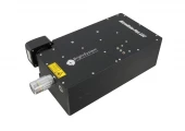
Description
The MicroMake 266 Laser Micromachining System by Bright System offers a comprehensive solution for high-precision microprocessing tasks. Engineered with a compact and integrated design, it encompasses all essential components required for direct laser microprocessing in a single monolithic unit.
With live microscope imaging capabilities, users can monitor samples throughout the machining process, ensuring precise results from alignment to quality checks. This versatile system is adept at various applications, including controlled ablation, microdrilling, precision cutting, selective material removal, and 3D microfabrication. Its adaptability makes it an ideal tool for industries ranging from microelectronics and biomedical devices to optical substrates and micromechanics. Tailored for OEM customers, the MicroMake 266 boasts a compact footprint and operates on low-voltage electrical power.
Moreover, it offers optional enhancements such as different objective lenses, an external control box, and an XYZ translation stage, catering to specific application needs. With its capability to deliver high peak power, it provides efficient laser microprocessing on a diverse range of materials, making it a reliable choice for demanding microengineering tasks.
MicroMake 266 Plus: Laser Micromachining System
Specifications
| Materials: | Metals, Thermoset Plastics, Thermoplastics, Polimers, Textile, Wood, Paper, Stones, Ceramics, Glass |
|---|---|
| Laser Type: | DPSS (Other) |
| Laser Wavelength: | 266 nm (Deep UV) |
| Laser Output Power: | 7000 W |
| Laser Safety: | Not classified |
| Work Area X: | 1 mm |
| Work Area Y: | 1 mm |
| Processing Speed: | 50 mm/sec |
| Features And Options: | Air-Cooled |
| Frequency: | 10-50 kHz |
| Lens Magnification: | 10x |
| Working Distance: | 20 mm |
| Spatial Resolution: | 3.0 µm |
| Overall Mechanical Dimensions: | 39x24x11 cm3 |
Got questions about specs? Use the inquiry form to ask.
 Download Data Sheet

Features
- Compact Laser Micromachining System: MicroMake by Bright System is an integrated, monolithic laser micromachining unit designed for high-precision microprocessing, microfabrication, laser ablation, microdrilling, cutting, and selective material removal.
- High-Precision Laser Ablation and Cutting: Enables programmable machining of arbitrary shapes for controlled ablation, precision cutting, surface texturing, microstructuring, and thin-film removal.
- Live Microscope Imaging During Processing: Built-in live imaging allows real-time sample alignment, process monitoring, and immediate quality inspection during laser machining operations.
- Down to 2 μm Laser Spot Size: Supports ultra-fine feature generation for demanding micromachining applications requiring high spatial resolution and excellent process control.
- Standard 1 mm Processing Area: Provides a practical micromachining field for high-resolution processing of wafers, masks, displays, PCBs, ceramic substrates, optical components, and biomedical parts.
- 532 nm and 266 nm Laser Options: Available with nanosecond and picosecond laser sources at 532 nm and 266 nm, enabling optimized processing across metals, ceramics, polymers, dielectrics, thin films, and transparent materials.
- Suitable for a Wide Range of Materials: Designed for precise laser processing of microelectronic substrates, metal films, ceramic substrates, optical materials, transparent dielectrics, biomedical devices, and micromechanical components.
- Direct 3D Microstructuring Capability: Supports advanced 3D direct laser microfabrication for functional microfeatures, microtextures, and high-resolution surface modifications.
- Precision Surface Texturing: Ideal for creating controlled microtextures to modify surface properties, improve functionality, or produce engineered surface patterns.
- PCB Track Interruption and Repair: Enables selective interruption of conductive tracks and microwires on printed circuit boards and microelectronic devices for correction, trimming, and failure analysis.
- Microcoding for Anti-Counterfeiting: Suitable for permanent micro-marking and microcoding on small components, substrates, and devices for traceability, authentication, and anti-counterfeiting applications.
- Thin Film Removal on Hard Substrates: Provides accurate removal of thin films from hard materials while minimizing damage to the underlying substrate.
- Selective Metal Removal on Ceramic Substrates: Designed for high-precision removal of metal layers from ceramic substrates used in electronics, sensors, and advanced manufacturing.
- Microcorrection of Wafers, Masks, and Displays: Supports defect correction and localized modification on wafers, photomasks, display panels, and other high-value microfabricated components.
- Microdrilling on Metals and Transparent Dielectrics: Capable of calibrated laser microdrilling for medical devices, precision components, metals, glass-like materials, and transparent dielectric substrates.
- Embedded Illumination Unit: Integrated illumination improves visibility, alignment accuracy, and inspection quality during micromachining operations.
- Objective Lens Flexibility: Supplied with a standard 10X objective lens, with additional objective lenses available to adapt the system for different spot sizes, fields of view, and processing requirements.
- High-Speed USB Camera Option: Optional high-speed, high-resolution USB camera enables enhanced live monitoring, alignment, documentation, and process verification.
- Optional XYZ Translation Stage: Available with manual or motorized XY and Z stages for precise sample positioning and expanded processing flexibility.
- Typical 120 mm XY Travel: Optional XY manual or motorized stage provides large-area positioning capability for samples, devices, and substrates.
- Typical 40 mm Z Travel: Optional Z manual or motorized stage supports accurate focus adjustment and processing of components with varying thicknesses.
- OEM-Ready Compact Design: The compact footprint and single low-voltage power requirement make MicroMake well suited for OEM integration into automated production, inspection, and repair systems.
- Ready-to-Use Workstation Configuration: Available as a table-top laser micromachining workstation with external mounts, manual stages, AC power supply unit, and optional safety enclosure.
- Class 1 Safety Enclosure Option: Optional Class 1 laser safe
Applications
- Laser micromachining and microfabrication: high-precision machining of miniature components, complex microfeatures, and programmable arbitrary shapes with micron-level accuracy.
- 3D direct microstructuring: fabrication of three-dimensional microstructures, functional surface profiles, cavities, channels, and patterned features on a wide range of materials.
- Precision laser ablation: controlled material removal for research, prototyping, product development, and small-scale production applications.
- Laser microcutting: fine cutting of thin foils, films, metals, ceramics, polymers, glass, and other technical materials requiring narrow kerf widths and high edge quality.
- Laser microdrilling: calibrated drilling of microholes in metals, transparent dielectrics, medical devices, sensors, microfluidic components, and precision mechanical parts.
- Surface texturing and functionalization: creation of precision microtextures for improved adhesion, wettability control, friction reduction, tribology studies, optical effects, and biomedical surface modification.
- PCB track interruption and circuit repair: selective cutting, trimming, and interruption of conductive tracks on printed circuit boards, flexible circuits, and microelectronic assemblies.
- Selective metal removal: localized removal of metal layers from ceramic substrates, glass substrates, wafers, masks, and electronic devices without excessive damage to the underlying material.
- Thin film patterning and removal: precise structuring or stripping of thin films on hard substrates, including coated glass, ceramics, semiconductors, and display-related materials.
- Microcorrection of wafers, masks, and displays: repair and correction of defects on semiconductor wafers, photomasks, metal masks, display panels, and microelectronic components.
- Metal mask defect correction: localized ablation and repair of metal mask defects for microelectronics, displays, and precision patterning applications.
- Microwire interruption: selective interruption of fine wires, conductive paths, and microconnections for electronics testing, sensor development, and device trimming.
- Anti-counterfeiting microcoding: laser marking, micro-engraving, and coding of security features, identification marks, serial numbers, QR-style microcodes, and traceability patterns.
- Biomedical device micromachining: precision drilling, cutting, texturing, and marking of medical components, implants, surgical tools, diagnostic devices, and microfluidic biomedical structures.
- Microfluidics fabrication: creation of microchannels, ports, reservoirs, and access holes in glass, polymers, ceramics, and transparent dielectric materials.
- Optical substrate processing: micromachining of optical glass, coated optics, transparent dielectrics, and functional optical surfaces for photonics and optoelectronics applications.
- Semiconductor and MEMS processing: localized laser trimming, patterning, ablation, wafer correction, mask repair, and microfeature generation for semiconductor devices and MEMS components.
- Display manufacturing and repair: microcorrection, thin film removal, conductive layer patterning, and defect repair for flat-panel displays and related display technologies.
- Sensor and microsystem fabrication: precise structuring, drilling, trimming, and marking of sensor substrates, microelectrodes, ceramic packages, and miniaturized device components.
- Micromechanics and precision manufacturing: production of fine mechanical features, slots, holes, grooves, and miniature parts for watches, instruments, aerospace components, and high-value engineering devices.
- R&D laser processing workstation: ideal for laboratories, universities, research centers, and development teams requiring flexible laser ablation, cutting, drilling, and imaging in a compact system.
- OEM integration for laser microprocessing: compact laser micromachining module suitable for integration into custom production platforms, automated inspection systems, and specialized manufacturing tools.
Frequently Asked Questions
What materials can the MicroMake 266 Laser Micromachining System work with?
What are the typical applications of the MicroMake 266 system?
Does the MicroMake 266 system offer live imaging during the machining process?
What are the optional enhancements available for the MicroMake 266 system?
Is the MicroMake 266 system suitable for OEM customers?
Got more questions? Use the inquiry form to ask the supplier directly.
Similar Products
Your inquiry has been received.
Create an account by adding a password
Why create an account?
- Auto-complete inquiry forms
- View and manage all your past messages
- Save products to your favorites
- Close your account anytime — no hassle