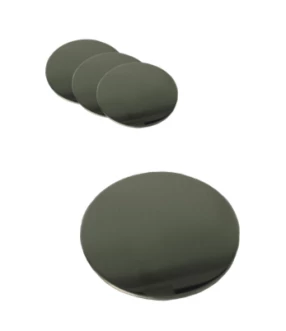
Germanium And Silicon Wafers
Description
These custom wafers can have non-standard diameters or thickness, laser marking, flats, chemical etching, etc... Test or Mechanical grade Wafers We supply test/monitor wafers, or monitor wafers for testing semiconductor fabrication lines and processes. We put prime polished wafers through a sophisticated chemical-mechanical polishing process and package in clean rooms.
Germanium And Silicon Wafers
Specifications |
|
|---|---|
| Wafer Material: | Silicon (Si), Germanium (Ge) |
| Diameter: | 15-150 mm |
| Thickness: | 0.3-5 um |
For pricing, technical or any other questions please contact the supplier
- No registration required
- No markups, no fees
- Direct contact with supplier
-
Ships from:
United States
-
Sold by:
-
On FindLight:
External Vendor

Claim Novotech Inc Page to edit and add data
Frequently Asked Questions
Yes, the wafers can be customized according to specific requirements such as non-standard diameters or thickness, laser marking, flats, chemical etching, etc.
Germanium and Silicon wafers are used in the semiconductor industry for the production of electronic components such as transistors, diodes, and integrated circuits.
The resistivity range of the wafers is 0.005ohm.cm to 20,000ohm.cm.
The standard diameter of the wafers is 15mm to 150mm, and the thickness ranges from 0.3mm to 5mm.
The TTV is less than 0.015mm, BOW is less than 0.015mm, and WARP is less than 0.015mm.