

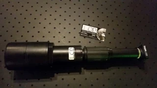
Description
Micron Laser Technology (MLT) stands at the forefront of laser services for the printed circuit board (PCB) industry, offering a comprehensive range of solutions from single-sided to multi-layer, rigid, and flexible circuits. As a trusted partner for circuit board manufacturers, MLT provides cost-effective, outsourced laser services that enhance product technology and deliver a competitive edge. By leveraging advanced laser material processing, MLT ensures precision and efficiency in every project, making it an integral part of the manufacturing process.
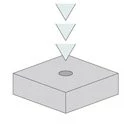
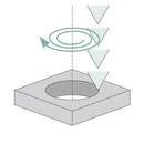
One of the key offerings from MLT is its microvia laser drilling services, which cater to both copper clad and unclad laminates. These services adhere to IPC high-density interconnect standards, with laser vias produced to a minimum diameter of 30 micrometers. This precision ensures that manufacturers can meet the demands of modern electronic designs with confidence and reliability.
MLT's laser routing services are another highlight, providing cutting-edge solutions with tolerances as fine as 25 micrometers or better. This service minimizes visual discoloration and eliminates mechanical stresses, offering radius-free internal edge profiles without the need for expensive dies and punches. Such precision and efficiency make MLT's laser routing an invaluable asset for manufacturers looking to optimize their production processes.
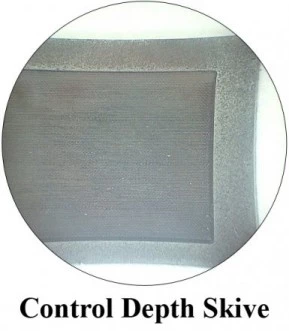
In addition to drilling and routing, MLT offers laser skiving services, which allow for controlled material removal to a specific depth or targeted layer. This capability is essential for applications requiring cavity formation, floating contacts, and selective solder mask removal, among others. MLT's expertise in laser skiving ensures that manufacturers can achieve the desired material configurations with precision and minimal waste.
MLT also excels in PCB laser rework, providing precision rework and recovery services to minimize scrap and ensure timely deliveries. This includes solder mask removal, pad isolation, and trace trimming, among other services. By offering such comprehensive rework solutions, MLT helps manufacturers maintain high-quality standards and reduce production costs.
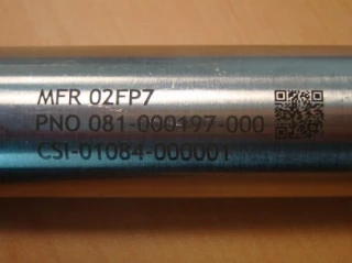
Finally, MLT's laser marking services utilize both ultraviolet and infrared lasers to produce permanent, high-resolution, non-contact markings, logos, barcodes, and serialization. These markings comply with standards such as MIL-STD-130M for defense and SEMI M12/M13 for semiconductors, ensuring that products meet industry requirements.
Laser Drilling
Specifications
| Type Of Service: | Engineering design |
|---|---|
| Minimum Laser Via Diameter: | 30um |
| Laser Routing Tolerances: | 25um or better |
| Infrared (CO2) Positional And Dimensional Tolerances: | +/-.002” (50um) |
| Ultraviolet (UV) Positional And Dimensional Tolerances: | +/-.001” (25um) |
| Serialization Tolerance: | Up to 10um |
Got questions about specs? Use the inquiry form to ask.
Features
- Comprehensive PCB Laser Services: From single-sided to multi-layer, rigid and flexible circuits, MLT offers a cost-effective, outsourced solution for circuit board manufacturers.
- Microvia Drilling: Provides laser drilling for copper clad and unclad laminates to IPC high density interconnect standards, with laser vias as small as 30um in diameter.
- Laser Routing: Achieve 25um or better tolerances with minimal visual discoloration, radius-free internal edge profiles, and no mechanical stresses. Ideal for applications like excising, depaneling, and thermal management preforms.
- Laser Skiving: Allows for controlled material removal to a limited depth or targeted layer, suitable for cavity formation, floating contacts, and selective soldermask removal.
- PCB Laser Rework: Precision laser rework services to minimize scrap and ensure timely deliveries, including solder mask removal and BGA decapsulation.
- Laser Marking, Barcodes, and Serialization: High-resolution, non-contact markings compliant with MIL-STD-130M and SEMI M12/M13 standards.
- Laser Service Advantages: Offers positional and dimensional tolerances with infrared (CO2) at +/-.002” (50um) and ultraviolet (UV) at +/-.001” (25um).
- Diverse PCB Materials: Compatible with a wide range of materials including FR4, Isola, Rogers, Duroid, Teflon, and more.
- Advanced Technology: MLT's advanced laser material processing provides a competitive edge and enhances product technology.
- Industry Standards: AS9100 Certified and ITAR Registered, ensuring high-quality and compliant services.
Applications
- HDI PCB Manufacturing: Supports blind, buried, stacked, and through-via configurations.
- Depaneling & Routing: Ideal for excising circuits, scoring, or connector profiling without mechanical stress.
- Cavity & Isolation Features: Enables cavity formation, floating contacts, and buried pad exposure.
- PCB Rework & Repair: Minimizes scrap by reworking soldermask, gold shorts, or BGA decapsulation.
- Product Identification: Delivers compliant marking, serialization, and traceability for electronics and defense industries.
Frequently Asked Questions
What are the dimensional and positional tolerances achieved through laser drilling?
What are the factors that contribute to hole quality in laser drilling?
What is laser drilling used for?
What services does MLT offer for PCB laser processing?
What wavelengths are used in MLT laser drilling processes?
Got more questions? Use the RFQ form to ask the supplier directly.
Similar Products


Need pricing for this product? Send a quick inquiry
Your inquiry has been received.
Create an account by adding a password
Why create an account?
- Auto-complete inquiry forms
- View and manage all your past messages
- Save products to your favorites
- Close your account anytime — no hassle