
Description
Micron Laser Technology (MLT) stands as a premier provider of laser services for the printed circuit board industry. Offering a comprehensive range of PCB laser services, MLT caters to the needs of circuit board manufacturers seeking cost-effective, outsourced solutions. From single-sided to multi-layer, rigid, and flexible circuits, MLT's advanced laser material processing not only enhances product technology but also provides a competitive edge in the market. As an integral manufacturing partner, MLT ensures precision and quality in every project.
One of the standout services offered by MLT is microvia laser drilling. This process is meticulously designed to meet IPC high-density interconnect standards, accommodating both copper-clad and unclad laminates. With the capability to produce laser vias with a minimum diameter of 30 micrometers, MLT ensures that even the most intricate designs are executed with precision. This level of detail is crucial for manufacturers aiming to achieve high-performance circuit boards.
MLT's expertise extends to PCB laser routing, a service characterized by its precision and efficiency. With tolerances of 25 micrometers or better, MLT's laser routing services minimize visual discoloration and eliminate mechanical stresses, ensuring clean and precise cuts without the need for expensive dies and punches. This service is ideal for applications requiring intricate designs and high-quality finishes.
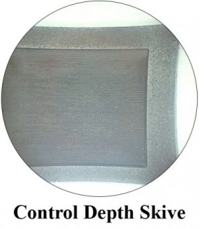
In addition to drilling and routing, MLT offers laser skiving services, which allow for controlled material removal to a specific depth or targeted layer. This precision is essential for applications such as cavity formation and selective solder mask removal, where accuracy is paramount. MLT's laser skiving services ensure that manufacturers can achieve the desired specifications without compromising on quality.
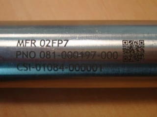
MLT also provides PCB laser rework services, offering a range of precision rework and recovery solutions for non-conforming products. This service is designed to minimize scrap and ensure timely deliveries, making it an invaluable resource for manufacturers facing production challenges. Furthermore, MLT's laser marking capabilities utilize both ultraviolet and infrared lasers to produce permanent, high-resolution markings, logos, barcodes, and serialization, compliant with industry standards such as MIL-STD-130M and SEMI M12/M13.
Overall, Micron Laser Technology's PCB laser services are a testament to their commitment to quality and innovation. By leveraging advanced laser technology, MLT provides circuit board manufacturers with the tools they need to excel in a competitive industry, ensuring precision, efficiency, and reliability in every project.
Laser Skiving
Specifications
| Type Of Service: | Engineering design |
|---|---|
| Minimum Laser Via Diameter: | 30 um |
| Laser Routing Tolerances: | 25 um or better |
| Infrared (CO2) Tolerances: | +/- .002” (50 um) |
| Ultraviolet (UV) Tolerances: | +/- .001” (25 um) |
| Serialization Tolerance: | Up to 10 um |
Got questions about specs? Use the inquiry form to ask.
Features
- Microvia Drilling: Produces vias down to 30 µm with IPC HDI compliance.
- High-Precision Routing: ±25 µm tolerances, radius-free edges, and no mechanical stresses.
- Laser Skiving: Controlled material removal for cavity formation and selective layer access.
- Laser Rework: Restores non-conforming boards, reducing scrap and improving yields.
- Laser Marking: Permanent barcodes, serialization, and logos compliant with defense and semiconductor standards.
- Versatile Material Compatibility: Processes FR4, polyimide, PTFE, ceramics, and advanced composites.
- Certified Quality: AS9100C and ISO9001 certified, ITAR registered, ensuring aerospace-grade compliance.
- Fast Turnaround: Same-day services available for production overflow.
Applications
- HDI PCB Fabrication: Microvia drilling and stacked via formation for advanced interconnects.
- Depaneling and Routing: Precision excising of boards, connectors, and scoring operations.
- Cavity Formation & Isolation: Controlled skiving for buried pads, floating contacts, and soldermask removal.
- PCB Rework & Recovery: Salvaging non-conforming products through selective material removal.
- Component & Product Marking: Permanent barcodes, serialization, and logos for traceability.
- Aerospace and Defense Electronics: ITAR-compliant processing for mission-critical applications.
Frequently Asked Questions
How does laser skiving work?
What are some applications of laser skiving?
What are the positional and dimensional tolerances of laser service?
What is control depth skiving?
What is laser skiving?
Got more questions? Use the RFQ form to ask the supplier directly.
Similar Products


Need pricing for this product? Send a quick inquiry
Your inquiry has been received.
Create an account by adding a password
Why create an account?
- Auto-complete inquiry forms
- View and manage all your past messages
- Save products to your favorites
- Close your account anytime — no hassle