Description
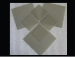
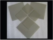
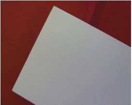
Accuratus is renowned for its inventory of standard aluminum nitride substrates, ensuring rapid delivery to meet urgent requirements. These substrates are available in industry-standard thicknesses of 0.025 inches and 0.040 inches, making them suitable for a variety of applications. Our commitment to quality and efficiency means you can expect prompt responses to your inquiries. For a quotation, feel free to call us at 908-213-7070 or send a fax to 908-213-7069. Alternatively, you can submit your request for a quote through our online platform.
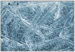
Our aluminum nitride substrates are manufactured using either tape casting or dry pressing methods. Tape casting allows for production of substrates up to 5 inches by 7 inches and 0.060 inches thick, while dry pressing can produce substrates up to 2 inches square and 0.250 inches thick. These methods ensure strong substrates with consistent material properties, boasting at least 170W/m°K room temperature thermal conductivity. For those requiring higher thermal conductivity, specialized methods can achieve up to 200 W/m°K, albeit with reduced mechanical strength.
Accuratus substrates are delivered ready for use, but they also offer flexibility for further processing. They are compatible with a range of processes including mechanical dicing, laser scribing and cutting, thick film hybrid metallizing, thick film refractory metallizing, thin film metallizing, and direct bond copper processes. This versatility ensures that our substrates can be tailored to meet specific project needs.
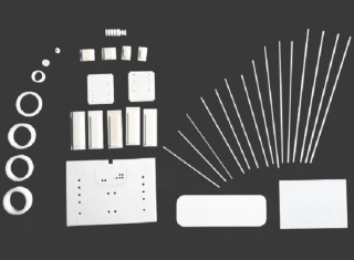
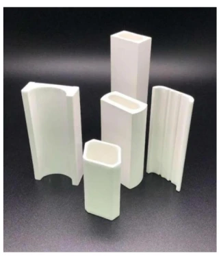
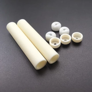
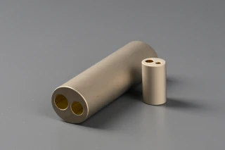
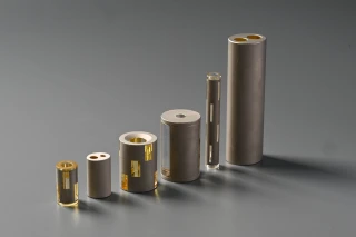
In addition to substrates, Accuratus provides isostatically pressed aluminum nitride components. Available in various forms such as bars, rods, and tiles, these components can have cross sections up to 2 inches and lengths up to 8 inches. Post-firing, these components are typically precision machined to adhere to specific customer dimensional requirements. The typical material properties for these components can be found on the Aluminum Nitride page under the Materials section on our website.
Aluminum Nitride Substrates and Components
Specifications
| Material: | Aluminum Nitride |
|---|---|
| Type Of Ceramic: | Not Applicable |
| Component Type: | Substrates |
| Standard Thickness: | 0.025 inches |
| Standard Thickness: | 0.040 inches |
| Tape Casting Size: | 5 inches by 7 inches |
| Tape Casting Thickness: | 0.060 inches |
| Dry Pressing Size: | 2 inches square |
| Dry Pressing Thickness: | 0.250 inches |
| Standard Thermal Conductivity: | 170 W/m°K |
| Specialized Thermal Conductivity: | 200 W/m°K |
| Isostatically Pressed Component Cross Section: | 2 inches |
| Isostatically Pressed Component Length: | 8 inches |
Got questions about specs? Use the inquiry form to ask.
Features
- High Thermal Conductivity: Standard substrates provide at least 170 W/m°K thermal conductivity, with specialized methods achieving up to 200 W/m°K.
- Low Thermal Expansion: Ensures stability and reliability in various applications.
- Dielectric Properties: Suitable for applications requiring electrical insulation.
- Cost-Effective: Offers a balance of performance and affordability.
- Fast Delivery: Inventory of standard sizes ensures quick fulfillment of orders.
- Variety of Sizes: Tape casting produces substrates up to 5 inches by 7 inches and .060 inches thick, while dry pressing allows for sizes up to 2 inches square and .250 inches thick.
- Versatile Processing Compatibility: Ready for mechanical dicing, laser scribing, cutting, and various metallizing processes.
- Custom Components: Isostatically pressed aluminum nitride components available in bars, rods, and tiles with up to 2-inch cross section and 8-inch length, precision-machined to specifications.
Applications
- Power Electronics: Ideal for substrates in high-power circuits requiring efficient heat dissipation.
- LED Packaging: Provides thermal management and electrical insulation for high-brightness LEDs.
- RF and Microwave Devices: Supports high-frequency components with stable thermal properties.
- Optoelectronic Modules: Suitable for laser diode and photonic device mounting.
- Thick and Thin Film Circuits: Compatible with hybrid circuit metallization processes.
- Direct Bond Copper Applications: Enables direct copper bonding for advanced packaging solutions.
Frequently Asked Questions
What are the standard thicknesses of the aluminum nitride substrates?
What are the methods used to produce the aluminum nitride substrates?
What are the compatible processes for the aluminum nitride substrates?
What are the characteristics of the aluminum nitride substrates?
What are the available sizes for the aluminum nitride components?
Got more questions? Use the RFQ form to ask the supplier directly.
Similar Products

Need pricing for this product? Send a quick inquiry
Your inquiry has been received.
Create an account by adding a password
Why create an account?
- Auto-complete inquiry forms
- View and manage all your past messages
- Save products to your favorites
- Close your account anytime — no hassle