


Description
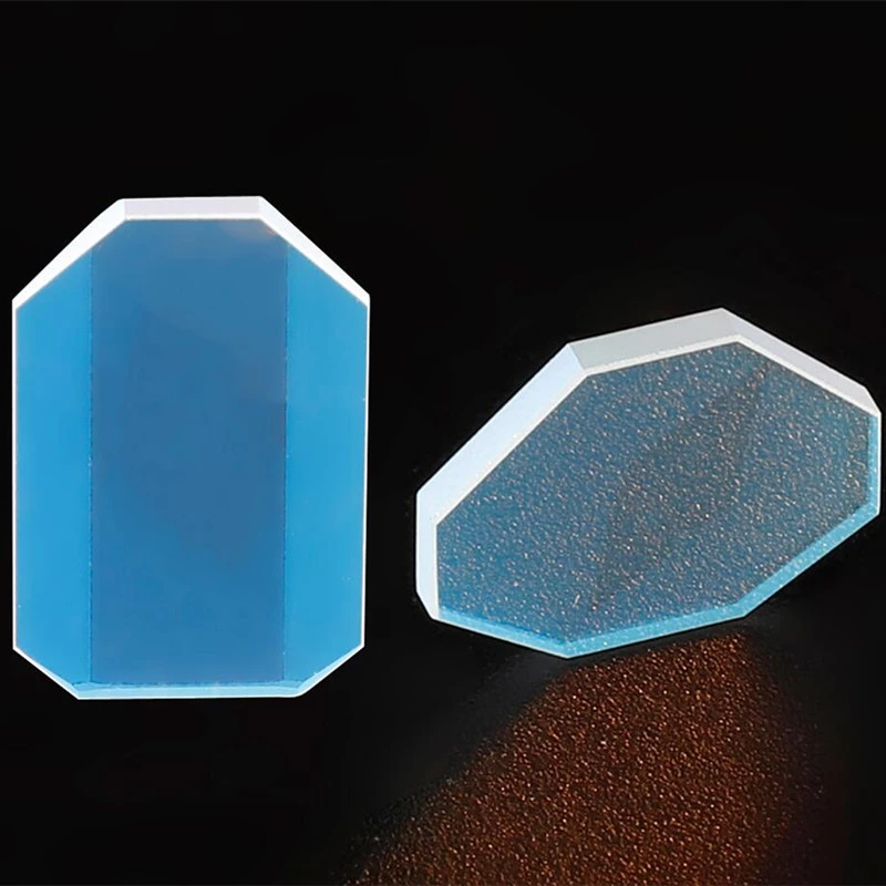
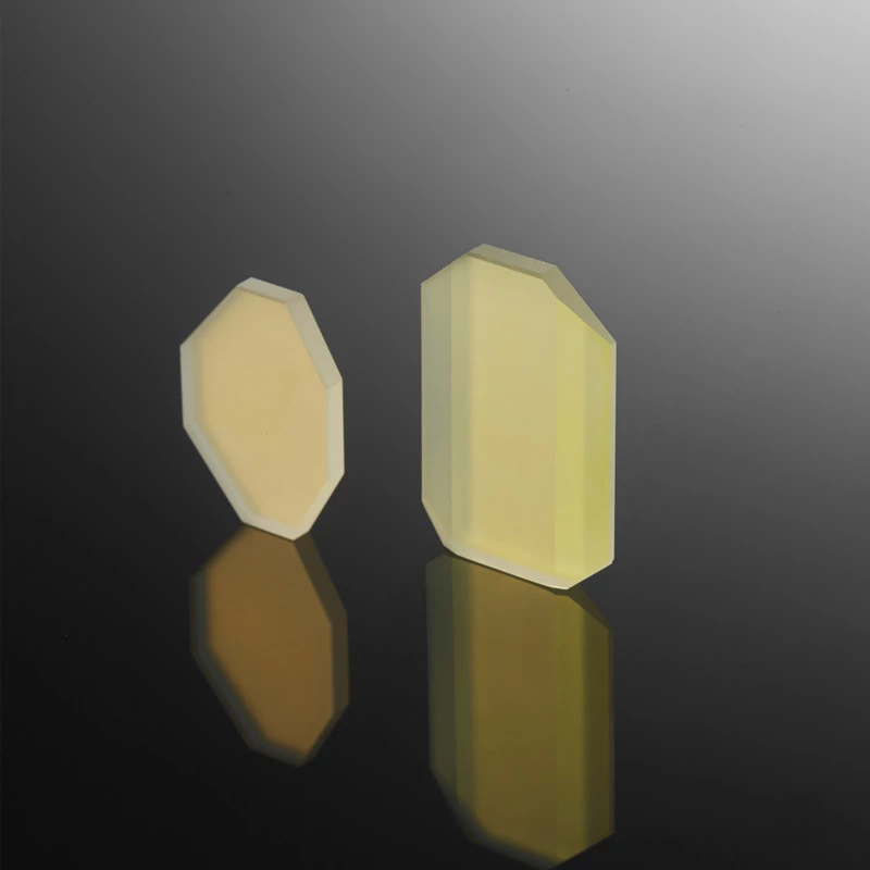
Dielectric-coated scanning mirrors based on fused silica substrates are high-precision optical components designed for fast and accurate laser beam steering in demanding scanning systems. These mirrors are widely used in laser processing, imaging, and measurement applications where optical stability, high reflectivity, and low thermal distortion are critical.
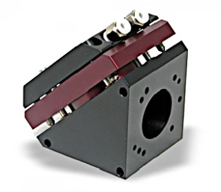
Custom 1064nm Fused Silica Scanning Mirror with Dielectric Coating
Specifications
| Type: | Mirror |
|---|---|
| Compatibility: | Other / Not specified |
| Build Material: | Fused Silica |
| Beam Diameter: | 10mm |
| Size: | 18.3*13*2mm |
| Dimension Tolerance: | +0.0/-0.1mm |
| Wavelength: | 1064nm |
| Coating: | Dielectric Coating |
| Surface Quality: | 60-40, 40-20, or better |
| Surface Flatness: | λ/4 or better |
Got questions about specs? Use the inquiry form to ask.
Features
- Ultra-Low Thermal Expansion & High Stability: Adopts fused silica substrate with inherent ultra-low thermal expansion performance, which can maintain structural stability under temperature fluctuations and avoid deformation during long-term operation, ensuring consistent scanning accuracy
- High-Power Laser Tolerance: Equipped with multi-layer dielectric coating that features excellent laser damage resistance, enabling stable operation in high-power laser scenarios (both pulsed and continuous-wave) without coating failure or performance degradation
- Ultra-High Reflectivity & Low Optical Loss: Customized multi-layer dielectric coating design achieves ultra-high reflectivity at target wavelengths, minimizing laser energy loss and ensuring efficient beam transmission and utilization
- Broad Wavelength Adaptability: The dielectric coating can be customized according to application requirements, adapting to ultraviolet, visible and near-infrared wavelength bands, and meeting the needs of diverse laser scanning scenarios
- Excellent Environmental Durability: The dielectric coating has inherent corrosion resistance and anti-tarnishing properties, and the fused silica substrate is chemically stable, making the product suitable for long-term operation in harsh environments such as industrial sites and scientific research laboratories
- Flexible Customization: Supports personalized customization according to actual application needs, including substrate size, shape, clear aperture and coating parameters, to perfectly match different scanning system configurations
Applications
- High-Power Laser Marking & Engraving: Ideal for fiber laser (1064 nm) and green laser (532 nm) marking systems used in electronics, automotive, and jewelry manufacturing, ensuring high-precision and high-speed marking
- Ultraviolet Laser Micromachining: Suitable for 355 nm UV laser micromachining systems in semiconductor wafer processing, PCB drilling, and micro-electromechanical systems (MEMS) fabrication, leveraging the fused silica substrate's UV transmittance and coating's high UV reflectivity
- 3D Printing & Additive Manufacturing: Used in high-precision 3D printing systems (e.g., SLA, SLM) to control laser beam scanning trajectories, ensuring uniform material curing and high-quality print results
- Semiconductor Lithography & Inspection: Applied in semiconductor lithography scanners and wafer inspection systems, where ultra-high precision and thermal stability are critical for ensuring chip manufacturing accuracy
- Scientific Research & Laser Spectroscopy: Suitable for laser experimental setups, spectral analysis systems, and laser ranging equipment in academic and industrial research institutions, supporting high-precision optical measurements
- Medical Laser Systems: Used in ophthalmic laser surgery, dermatological laser treatment, and other medical laser devices, benefiting from the mirror's high biocompatibility, stability, and low optical loss
Frequently Asked Questions
What is the working principle of scanning mirror?
The working principle is that the laser beam is first incident on the X-axis galvanometer, and then incident on the Y-axis galvanometer. After secondary reflection by the Y-axis galvanometer, it can be projected onto the working plane to form a scanning point. Then the galvanometer motor drives the deflection of the beam deflector composed of the X and Y scanning heads to realize the movement of the laser beam within the predetermined scanning range, so that the laser focus point with a certain power density leaves a permanent mark on the marking material. mark to complete the scanning of the image.
What are the common substrates for scanning mirrors?
Common substrates include fused silica and silicon. Each is selected based on application requirements such as thermal stability, wavelength adaptability and environmental resistance.
Why is fused silica a preferred substrate for high-precision scanning mirrors?
Fused silica has inherent ultra-low thermal expansion, excellent optical uniformity and good chemical stability, which can maintain scanning accuracy under temperature fluctuations and harsh working conditions.
How to choose between metal coating and dielectric coating for scanning mirrors?
Choose metal coatings for broad wavelength coverage needs; select dielectric coatings when high reflectivity, low optical loss and high laser damage resistance are required for specific wavelengths.
Can UM Optics customize scanning mirrors with specific substrate and coating?
Yes. UM Optics provides customized services for scanning mirrors, which can tailor substrate materials (e.g., fused silica, silicon) and coating systems (e.g., metal, dielectric coatings) according to customers' specific application requirements.
Got more questions? Use the RFQ form to ask the supplier directly.
Similar Products
Need pricing for this product? Send a quick inquiry
Thank You!
Your inquiry has been received.
Create an account by adding a password
Why create an account?
- Auto-complete inquiry forms
- View and manage all your past messages
- Save products to your favorites
- Close your account anytime — no hassle