
Optical I/O for GPUs is the topic of this blog article
The explosive growth of artificial intelligence has fundamentally changed the requirements for modern computing infrastructure. Training large language models (LLMs), running generative AI systems, and supporting hyperscale inference workloads demand unprecedented computational power and data movement. While GPUs have become the engines driving AI innovation, a less visible bottleneck is rapidly emerging: the limitations of traditional electrical interconnects.
As GPU performance scales dramatically, the ability to move data efficiently between processors, memory, switches, and servers has become one of the most critical challenges in AI infrastructure. Copper-based electrical connections that served previous generations of computing are increasingly struggling to keep pace with the bandwidth, power, and thermal demands of next-generation AI systems.
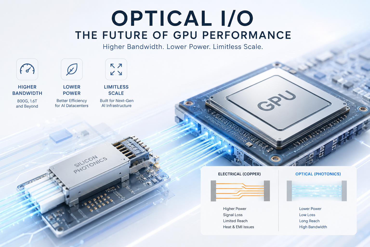
This challenge is accelerating interest in optical I/O, a technology that replaces conventional electrical interconnects with high-speed optical links. By leveraging silicon photonics, advanced modulators, integrated lasers, and optical fibers, optical I/O promises to dramatically improve bandwidth density, reduce power consumption, and enable the next era of scalable AI computing.
This article is brought to you by LECC Technology
The AI Bandwidth Explosion
Modern AI models require extraordinary amounts of data movement. In many cases, the computational capability of GPUs is no longer the primary limitation. Instead, communication between GPUs and memory subsystems has become a major constraint on overall system performance.
Training advanced AI models often involves thousands or even tens of thousands of GPUs working simultaneously in massive distributed clusters. These systems continuously exchange enormous volumes of data, including model parameters, gradients, activation maps, and synchronization signals.
High-performance GPU architectures now rely heavily on:
- high-bandwidth memory (HBM)
- GPU-to-GPU interconnects
- high-speed switch fabrics
- rack-scale networking
- ultra-low-latency communication
AI workloads place especially intense pressure on interconnect bandwidth because modern models are becoming both larger and more distributed. As parameter counts grow into the trillions, the amount of communication required between computing nodes rises dramatically.
Companies such as NVIDIA are already pushing the limits of existing interconnect technologies with advanced solutions like NVLink and NVSwitch. However, even these sophisticated electrical systems face growing physical constraints as data rates continue to increase.
The industry is now moving toward 800G and 1.6T optical networking infrastructure, while future AI systems may require even higher bandwidth densities. Achieving such performance using conventional copper interconnects becomes increasingly difficult from both technical and economic perspectives.
Why Copper Interconnects Are Reaching Their Limits
For decades, electrical signaling over copper traces and cables has been the dominant method for moving data inside computing systems. However, electrical interconnects face several fundamental limitations at extremely high data rates.
One of the most significant problems is signal attenuation. As electrical signals travel through copper traces, they gradually lose strength due to resistive and dielectric losses. These losses increase sharply with higher frequencies and longer transmission distances.
At data rates approaching 224 Gbps per lane and beyond, maintaining signal integrity over copper becomes exceptionally challenging. Engineers must employ increasingly complex equalization schemes, retimers, and signal conditioning circuits to compensate for degradation.
Unfortunately, these solutions introduce additional:
- power consumption
- latency
- thermal load
- system complexity
- cost
Power efficiency has become especially critical in AI datacenters. Large GPU clusters already consume enormous amounts of electricity, and interconnect power is becoming a growing fraction of total system energy consumption.
Thermal management also presents major challenges. High-speed electrical links generate substantial heat, which increases cooling requirements and complicates system design. In dense AI servers, thermal constraints can significantly limit scalability.
Another issue is bandwidth density. Copper interconnects occupy considerable physical space, making it difficult to support the extremely high I/O densities required for future AI accelerators.
As AI infrastructure scales toward larger clusters and faster communication fabrics, the limitations of electrical interconnects are becoming increasingly difficult to overcome economically.
What Is Optical I/O?
Optical I/O replaces electrical data transmission with optical communication using light signals. Instead of sending electrical pulses through copper traces, information is converted into optical signals and transmitted through optical waveguides or fibers.
A typical optical I/O system includes:
- lasers
- optical modulators
- photonic integrated circuits (PICs)
- photodetectors
- optical fibers or waveguides
The process begins when electrical signals generated by a GPU or processor are converted into optical signals using modulators. These optical signals travel through fiber or integrated waveguides with extremely low loss and high bandwidth. At the receiving end, photodetectors convert the optical signals back into electrical data.
Optical communication offers several major advantages over electrical signaling:
- significantly lower transmission loss
- higher bandwidth capacity
- reduced electromagnetic interference
- lower power consumption over longer distances
- improved scalability
Because light can carry large amounts of information with minimal attenuation, optical interconnects are particularly attractive for AI systems requiring massive data movement.
Unlike copper, optical fibers can maintain signal quality over much longer distances without requiring power-hungry equalization or retiming circuitry. This enables more efficient communication between servers, racks, and even entire datacenter clusters.
Silicon Photonics and Co-Packaged Optics
One of the key technologies enabling optical I/O for GPUs is silicon photonics. Silicon photonics integrates optical components onto semiconductor chips using manufacturing techniques similar to those used in conventional CMOS fabrication.
Silicon photonic devices can include:
- waveguides
- modulators
- multiplexers
- photodetectors
- optical switches
This integration enables compact, scalable, and cost-effective optical communication systems compatible with modern semiconductor manufacturing.
Companies such as Intel, Broadcom, and TSMC are heavily investing in silicon photonics technologies for next-generation AI infrastructure.
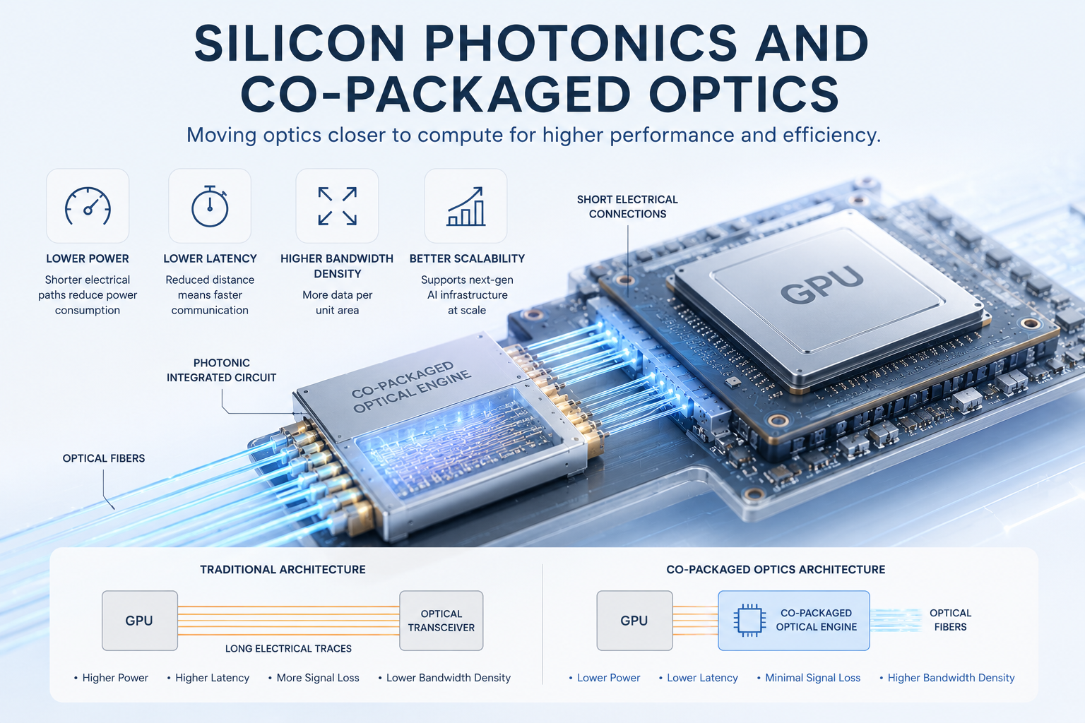
A particularly important development is co-packaged optics (CPO). In traditional systems, optical transceivers are located separately from processing chips. Co-packaged optics moves optical components much closer to GPUs or switch ASICs, dramatically reducing electrical trace lengths.
This architecture offers several advantages:
- lower power consumption
- reduced latency
- improved signal integrity
- higher bandwidth density
- better scalability
By minimizing long electrical paths, co-packaged optics helps overcome many of the limitations associated with high-speed copper signaling.
As AI systems continue scaling upward, co-packaged optics is increasingly viewed as a necessary step for maintaining practical power and performance levels.
Advanced Modulators and Thin-Film Lithium Niobate
Optical modulators are among the most critical components in optical I/O systems. These devices encode electrical data onto optical carriers by modulating properties such as intensity or phase.
Several modulation technologies are being explored for AI interconnects, including:
- Mach–Zehnder modulators
- ring resonator modulators
- electro-absorption modulators
- thin-film lithium niobate (TFLN) modulators
Thin-film lithium niobate has emerged as one of the most promising materials for high-speed optical communication. TFLN combines excellent electro-optic properties with compact device geometries and low power consumption.
Compared with traditional silicon modulators, TFLN devices can offer:
- higher bandwidth
- lower insertion loss
- lower drive voltage
- improved linearity
- better energy efficiency
These characteristics make TFLN especially attractive for future AI interconnects operating at extremely high data rates.
Researchers and startups such as Ayar Labs are developing advanced optical I/O architectures that integrate photonics directly with computing systems. Meanwhile, companies like Lightmatter are exploring broader photonic computing solutions aimed at AI acceleration.
Optical I/O for GPUs: Key Technical Challenges
Despite its enormous promise, optical I/O still faces several major technical and manufacturing challenges.
One of the biggest obstacles is packaging complexity. Optical alignment between fibers, waveguides, lasers, and photonic chips requires extremely high precision. Small alignment errors can significantly degrade optical coupling efficiency.
Thermal management also remains difficult. Although optical links can reduce interconnect power, integrated lasers and photonic components still generate heat that must be managed carefully.
Laser integration presents another challenge. Silicon itself is not an efficient light emitter, so many silicon photonics systems rely on heterogeneous integration of III-V semiconductor lasers. Achieving reliable, scalable, and cost-effective laser integration remains an active area of development.
Reliability is equally important. AI datacenters require components capable of operating continuously for years under demanding environmental conditions. Ensuring long-term reliability for integrated photonic systems is critical for widespread adoption.
Cost is another consideration. While silicon photonics promises economies of scale, advanced packaging and integration techniques can still be expensive compared with mature electrical interconnect technologies.
Nevertheless, the growing demands of AI infrastructure are making these challenges increasingly worthwhile to solve.
The Future of AI Infrastructure Is Optical
The transition toward optical I/O for GPUs represents more than just an incremental improvement in interconnect technology. It may fundamentally reshape the architecture of future AI systems.
As bandwidth demands continue rising, optical communication is expected to move progressively closer to the compute core itself. Future systems may incorporate:
- optical chip-to-chip communication
- optical memory fabrics
- photonic switching
- optical backplanes
- fully optical rack-scale interconnects
Some researchers are even exploring optical neural networks and photonic AI accelerators capable of performing computation directly in the optical domain.
Although fully optical computing remains a long-term vision, optical I/O is already emerging as a practical and necessary technology for scaling AI infrastructure.
The AI revolution is no longer limited by transistor performance alone. Increasingly, success depends on how efficiently data can move through the system. In this environment, photonics is becoming one of the most important enabling technologies for next-generation computing.
As GPUs continue evolving toward higher performance and larger-scale deployment, optical I/O is poised to become a foundational component of future AI datacenters.


