
Thin-film lithium niobate modulators is the topic of this blog article.
This article is brought to you by Zolix Instruments
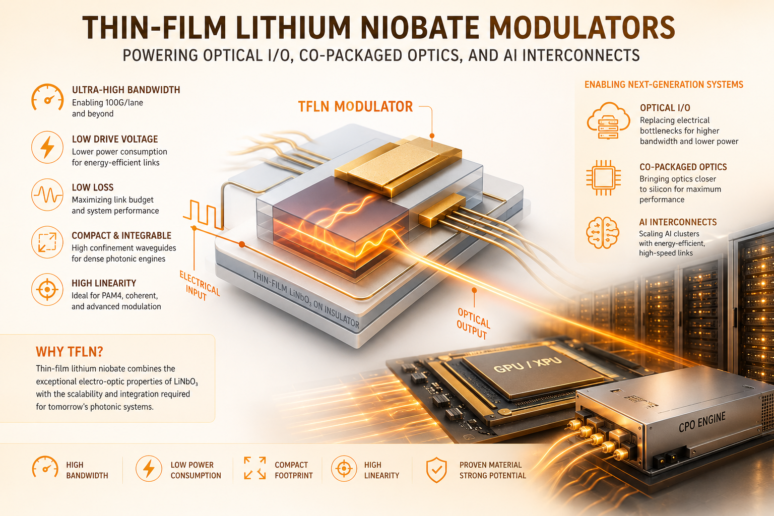
Artificial intelligence infrastructure is reshaping the requirements placed on interconnect hardware. Training clusters built around next-generation GPUs and XPUs are consuming more bandwidth, more power, and more rack space than traditional data-center architectures were designed to handle. As electrical links approach their limits in reach, signal integrity, and energy efficiency, optical interconnects are moving ever closer to the compute package. That shift is driving intense interest in optical I/O, co-packaged optics (CPO), and the photonic components that make these architectures possible.
Among those components, thin-film lithium niobate (TFLN) modulators are emerging as one of the most compelling technologies. Long valued in telecom for its electro-optic performance, lithium niobate has re-entered the spotlight in a new integrated form: ultra-thin films bonded onto insulating substrates and patterned into compact, high-confinement waveguides. The result is a modulator platform that combines the outstanding material properties of lithium niobate with the size, scalability, and integration potential demanded by modern photonic systems.
In this article, we examine why TFLN modulators matter for optical I/O and AI interconnects, how they compare with competing technologies, and where their real opportunities and limitations lie.
Why AI Interconnects Need Better Modulators
AI clusters stress interconnects in two ways at once: they require very high aggregate bandwidth and very low energy per transmitted bit. As GPU counts scale up and accelerator fabrics become denser, copper interconnects become increasingly problematic. Electrical links suffer from frequency-dependent loss, crosstalk, equalization overhead, and growing power dissipation as data rates climb. This is especially painful in short-reach but extremely bandwidth-hungry environments such as GPU-to-switch, accelerator-to-accelerator, and board-to-board interconnects.
Optical I/O aims to solve this by replacing some of the highest-stress electrical paths with optical links. In a co-packaged optics architecture, optical engines are brought physically closer to the switch ASIC or accelerator package, reducing electrical trace length and shifting the heavy bandwidth lifting to photonics. But this only works if the optical engine itself is compact, efficient, thermally manageable, and manufacturable at scale.
The modulator is central to that engine. It converts an electrical data stream into an optical one by changing the phase, intensity, or polarization of light. In data communications, the most common implementations are phase modulators and Mach–Zehnder modulators (MZMs), often operating with advanced modulation formats such as PAM4, QPSK, or coherent schemes depending on reach and architecture.
For optical I/O, the “ideal” modulator should offer:
- High electro-optic bandwidth for 100G/lane, 200G/lane, and beyond
- Low insertion loss to preserve optical link budget
- Low drive voltage for CMOS-friendly integration and reduced power
- Good linearity for multi-level or coherent modulation formats
- Compact footprint for dense photonic engines
- Stable performance over temperature
- Manufacturability compatible with volume packaging
This is where TFLN becomes interesting.
What Is Thin-Film Lithium Niobate?
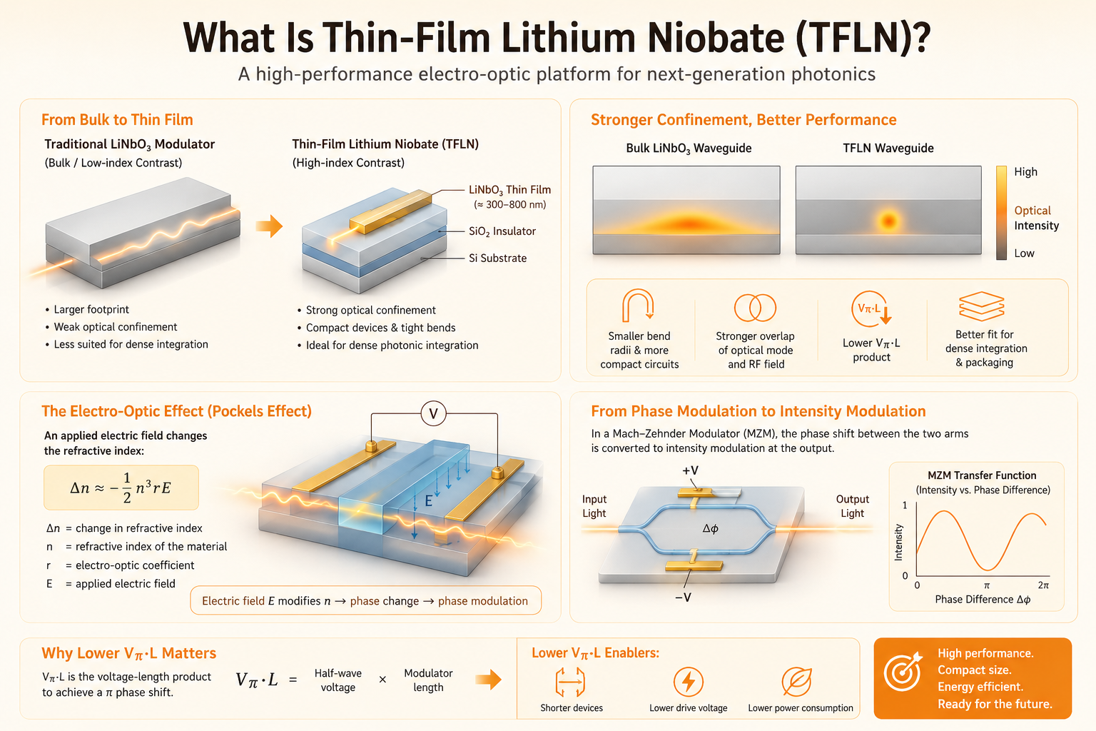
Lithium niobate (LiNbO3) has been a workhorse electro-optic material for decades. It offers a strong Pockels effect, wide optical transparency, good linearity, and mature understanding from telecom and microwave photonics. Traditional lithium niobate modulators, however, were often relatively large discrete devices based on low-index-contrast waveguides. They performed extremely well, but they were not naturally suited to dense photonic integration.
Thin-film lithium niobate changes that equation. In TFLN, a thin crystalline LiNbO3 layer—often on the order of a few hundred nanometers—is bonded onto an insulator substrate, typically silicon dioxide on silicon or a similar stack. Waveguides are then etched into the film, creating much stronger optical confinement than in legacy diffused lithium niobate devices.
That higher confinement delivers several benefits:
- Smaller bend radii and more compact photonic circuits
- Stronger overlap between the optical mode and RF electric field
- Lower Vπ·L product, enabling shorter devices or lower drive voltages
- Better compatibility with dense integration and hybrid photonic packaging
The electro-optic effect in lithium niobate is usually described through the linear Pockels relation, where the refractive index changes under an applied electric field. In simplified form:
Δn ≈ -(1/2) n^3 r E
where:
- Δn is the change in refractive index
- n is the refractive index of the material
- r is the relevant electro-optic coefficient
- E is the applied electric field
This refractive-index change creates phase modulation. In a Mach–Zehnder modulator, the optical phase shift between two arms is converted into intensity modulation at the output. The half-wave voltage-length product, commonly written as Vπ·L, is one of the key figures of merit. Lower Vπ·L generally means the device can achieve the required phase shift with less voltage, less length, or both.
Why Thin-Film Lithium Niobate Is Attractive for Optical I/O
TFLN modulators align well with several of the most important requirements in optical I/O and co-packaged optics.
High bandwidth with strong electro-optic efficiency
Lithium niobate has long been known for supporting very high-speed modulation. In thin-film form, optimized traveling-wave electrode designs and tight optical confinement have enabled TFLN modulators with bandwidths well beyond what legacy discrete platforms offered, while maintaining attractive Vπ values. This is critical as optical I/O moves toward 112 Gbaud, 224 Gbaud, and eventually higher lane rates.
A simplified bandwidth constraint for traveling-wave modulators is tied to RF-optical velocity matching and electrode loss. Although the full treatment is more involved, the design goal is straightforward: maximize overlap between the RF and optical fields while minimizing mismatch and microwave attenuation over the device length.
Lower drive voltage and improved energy efficiency
In AI interconnects, modulator power cannot be treated as a side issue. As the number of optical lanes rises, even modest inefficiencies become system-level thermal and power problems. TFLN’s lower Vπ·L relative to many traditional bulk lithium niobate designs makes it easier to reduce driver swing, shorten device length, or both.
For a simple capacitive view of switching energy, one often uses:
E_bit ≈ (1/4) C V^2
where:
- E_bit is energy per bit
- C is effective device capacitance
- V is the applied voltage swing
Real traveling-wave modulators are more complicated than a simple lumped capacitor, but the relationship still illustrates the design pressure: reducing required drive voltage helps reduce electrical energy consumption.
Low optical loss and high linearity
Optical I/O links must preserve as much optical power margin as possible, especially if external laser architectures, split optical power, or wavelength multiplexing are involved. TFLN waveguides have demonstrated low propagation loss and low excess loss in well-designed devices, which can translate into better link budgets.
Linearity also matters. Multi-level signaling and coherent modulation formats are sensitive to distortion. Lithium niobate has historically been attractive for analog photonics and microwave photonics precisely because of its linear electro-optic response. That heritage benefits high-performance datacom and optical compute-adjacent links as well.
Compactness without abandoning a proven material system
TFLN is attractive partly because it is not a brand-new electro-optic material with unknown reliability physics. It inherits a great deal from the lithium niobate ecosystem while addressing the footprint problem that limited older implementations. For co-packaged optics, this is an appealing middle ground: a material with known optical virtues, but in a form factor that fits integrated photonics.
TFLN vs Silicon Photonics and InP: Where It Fits
TFLN does not exist in a vacuum. Optical I/O platforms will be built from a mix of technologies, and in many cases hybrid integration rather than winner-take-all substitution will dominate.
The table below summarizes the broad trade space.
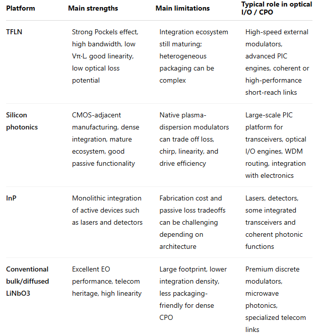
This comparison points to an important conclusion: TFLN is not necessarily trying to replace silicon photonics outright. Instead, it is increasingly viewed as a complementary high-performance modulation platform that can be heterogeneously integrated with silicon photonics, external lasers, drivers, and detectors.
In practice, a future optical I/O engine might use:
- silicon photonics for passive routing, splitters, multiplexers, and fiber attach structures
- TFLN for the modulator section
- InP or external laser sources for optical power generation
- CMOS/BiCMOS drivers and TIAs in adjacent electronics
Why Thin-Film Lithium Niobate Is Especially Interesting for Co-Packaged Optics
Co-packaged optics is not only about raw bandwidth. It is also about power density, signal integrity, thermal management, and packaging economics. A modulator technology that looks impressive in a lab demo but is difficult to package near hot ASICs or requires excessive drive voltage may struggle in deployment.
TFLN offers several features that map well onto CPO requirements:
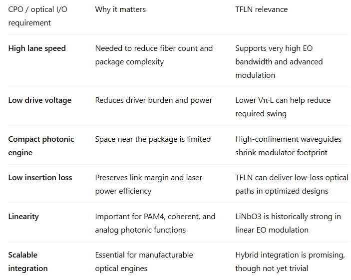
In other words, TFLN addresses several of the exact pain points that arise when optics moves from the pluggable module into the package-adjacent environment.
The Real Challenges: TFLN Is Promising, Not Magic
Despite the enthusiasm around TFLN, it is important to avoid oversimplifying the story. TFLN modulators are promising, but their success in optical I/O will depend as much on packaging and ecosystem maturity as on intrinsic material performance.
Heterogeneous integration complexity
Thin-film lithium niobate modulators are often only one piece of a larger photonic engine. The full system may also require lasers, multiplexers, photodiodes, RF drivers, thermal control, and fiber coupling. The more heterogeneous the stack becomes, the more challenging assembly, alignment, yield, and repairability become.
RF packaging and electrode design remain critical
A high-speed modulator is only as good as its microwave packaging. At the lane rates relevant to future AI interconnects, parasitics, impedance control, electrode loss, and co-design with the driver become central engineering problems. A beautiful modulator die does not guarantee a beautiful packaged optical engine.
Thermal and environmental reliability must be proven at scale
AI systems are not telecom central offices. Optical engines near switch ASICs or accelerators may face different thermal profiles, vibration environments, and maintenance expectations. Long-term reliability data, packaging robustness, and process consistency will matter greatly for qualification.
Cost and supply chain maturity still matter
Silicon photonics has an advantage in ecosystem scale, foundry familiarity, and integration mindshare. TFLN must continue to prove not only performance but also manufacturability, repeatability, and supply resilience if it is to become a mainstream optical I/O platform rather than a niche premium option.
What Markets Beyond AI Can Benefit?
Although AI interconnects are a major driver of attention, TFLN modulators are relevant far beyond optical I/O for GPUs. Their combination of high bandwidth, low loss, and strong linearity also makes them attractive for:
- Coherent telecom and datacom
- Microwave photonics and RF-over-fiber
- LiDAR and optical sensing
- Quantum photonics and frequency control
- High-speed test and measurement systems
- Analog optical links and photonic signal processing
That breadth is commercially important. It means investment in TFLN manufacturing and packaging can be supported by multiple adjacent markets rather than relying solely on AI infrastructure adoption.
Outlook: A Strong Candidate for the Optical I/O Era
Optical I/O and co-packaged optics are forcing the photonics industry to rethink the trade-offs between performance, power, density, and manufacturability. In that environment, thin-film lithium niobate stands out because it offers a rare combination of excellent electro-optic material properties and integrated-photonics-friendly scaling.
Thin-film lithium niobate modulators are not guaranteed to dominate every optical I/O architecture. Silicon photonics, InP, and hybrid platforms will all remain important. But TFLN is increasingly difficult to ignore. It addresses some of the most pressing needs of next-generation AI interconnects: high-speed modulation, lower drive voltage, strong linearity, and compact optical engines that can move photonics closer to the compute package.
For system architects, the most likely future is not a single universal material platform, but a layered ecosystem in which each technology is used where it performs best. In that ecosystem, thin-film lithium niobate modulators may become one of the enabling devices that help optical I/O move from compelling concept to deployable infrastructure.
As AI clusters continue to scale and the economics of electrical interconnects worsen, that possibility is becoming more than a research curiosity. It is becoming a market question with real urgency.


