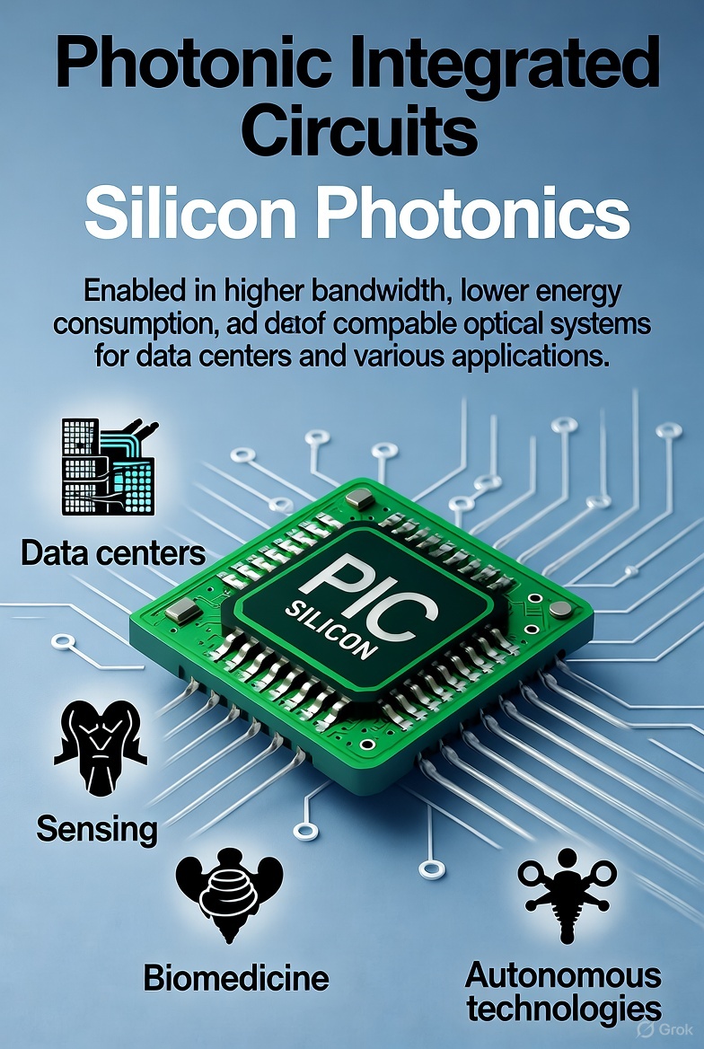
Photonic integrated circuits and silicon photonics is the subject of this blog article.
Introduction
As global data traffic soars, driven by AI workloads, cloud computing, and IoT systems, data centers are under immense pressure to deliver higher bandwidth with lower energy consumption. Electrical interconnects, the long-time backbone of data transmission, are now reaching their physical and thermal limits.
Enter Photonic Integrated Circuits (PICs), chips that manipulate light instead of electrons, and Silicon Photonics, a technology that leverages the vast semiconductor manufacturing ecosystem, to make photonic devices scalable and cost-effective.
Together, these two technologies are redefining how data moves, how sensors perceive, and how the next generation of computing infrastructure will be built.
What Are Photonic Integrated Circuits (PICs)?
Photonic Integrated Circuits are the optical analogs of electronic ICs. Instead of transistors and wires, PICs integrate lasers, modulators, waveguides, couplers, and detectors onto a single chip to process and transmit information using light.
Key material platforms include:
Indium Phosphide (InP): Ideal for active components such as lasers and amplifiers.
Silicon-on-Insulator (SOI): Perfect for high-density passive components and CMOS-compatible fabrication.
Silicon Nitride (SiN): Offers low-loss propagation, making it ideal for sensing and quantum photonics applications.
The result is a compact, stable, and scalable optical system capable of performing complex communication or sensing functions with exceptional speed and precision.
A typical PIC includes:
Waveguides for directing light signals,
Modulators for encoding data onto optical carriers,
Photodetectors for converting light back into electrical signals, and
Couplers and splitters for signal routing and distribution.
This integration dramatically reduces system footprint, cost, and power consumption compared to traditional discrete optical setups.
The Rise of Silicon Photonics
The term Silicon Photonics refers to using silicon as the medium for guiding and manipulating light. The attraction lies in its compatibility with CMOS processes, meaning optical and electronic components can be fabricated together using existing semiconductor infrastructure.
Over the past decade, silicon photonics has evolved from a research curiosity into a commercial reality. Breakthroughs in hybrid integration (bonding III–V materials onto silicon for laser sources) and wafer-level manufacturing have made it possible to mass-produce optical chips at scale.
Advantages of Silicon Photonics
CMOS Compatibility: Enables co-integration of photonics and electronics on the same chip, simplifying design and mass production.
Scalability: Fabrication on 200–300 mm wafers allows large-scale production with high yield.
Cost Efficiency: Leverages existing foundry infrastructure, reducing entry barriers for new technologies.
Wavelength Flexibility: Silicon’s transparency in the near-infrared region (1.3–1.55 µm) makes it ideal for optical communication applications.
Major players such as Intel, Cisco, IBM, and GlobalFoundries have invested heavily in this field, enabling 100G to 800G optical transceivers that now power hyperscale data centers.
Silicon photonics is no longer just about speed, it’s about energy efficiency, density, and cost reduction, enabling the data economy to continue scaling sustainably.
PICs in Data Centers: Solving the Bandwidth and Power Bottleneck
Modern data centers process vast volumes of information, with AI training models alone consuming megawatts of power. Electrical interconnects limited by copper’s resistance and heat dissipation are a major bottleneck. Global data center traffic continues to double roughly every 18–24 months. As AI workloads grow, energy consumption and signal latency have become major concerns.
Breaking the Copper Barrier
Copper interconnects, while inexpensive, struggle to carry signals over long distances at speeds beyond 100 Gbps without significant power loss and heat generation. In contrast, optical interconnects using PICs can:
Transmit data over kilometers with minimal loss,
Operate at terabit-per-second speeds, and
Significantly reduce electrical-to-optical conversion overhead.
Co-Packaged Optics (CPO) for Next-Gen Switches
To minimize latency and energy consumption, hyperscale operators like Meta, Google, and Microsoft are developing co-packaged optics, where PIC-based transceivers are integrated directly with switch ASICs. This architecture eliminates the need for long electrical traces, enabling ultra-low power consumption and higher bandwidth density, a critical step for AI and machine learning clusters.
Power and Sustainability
Data centers currently consume nearly 3% of the world’s total electricity. Transitioning to optical interconnects through silicon photonics could cut this power use by up to 40%, helping achieve sustainability targets without sacrificing performance.
Sensing Applications: From LIDAR to Biomedical Diagnostics
Beyond communications, PICs are revolutionizing optical sensing across industries from autonomous vehicles to environmental and biomedical monitoring.
1. LIDAR and 3D Mapping
Silicon photonics enables compact, solid-state LIDAR systems that can steer and detect laser beams without moving parts. Integrated photonic beam steering uses optical phased arrays, providing faster scanning speeds and greater durability for automotive and drone applications.
2. Environmental and Chemical Sensing
PIC-based integrated spectrometers and interferometers can detect trace gases and pollutants in real time. Their miniaturized form factor allows for distributed sensing networks in factories, agricultural fields, and urban environments.
3. Biomedical Diagnostics
Photonic biosensors integrated on silicon chips can identify DNA, proteins, or pathogens from microliter-scale samples. By using evanescent field interactions, these chips achieve extremely high sensitivity, ideal for point-of-care diagnostics, wearable health monitoring, and early disease detection.
4. Quantum and Neuromorphic Sensing
PICs are also being developed for quantum photonic circuits, where single photons act as qubits. Their high phase stability and small footprint make them suitable for quantum key distribution (QKD) and optical neural networks, representing a fusion of communication, sensing, and computing in one platform.
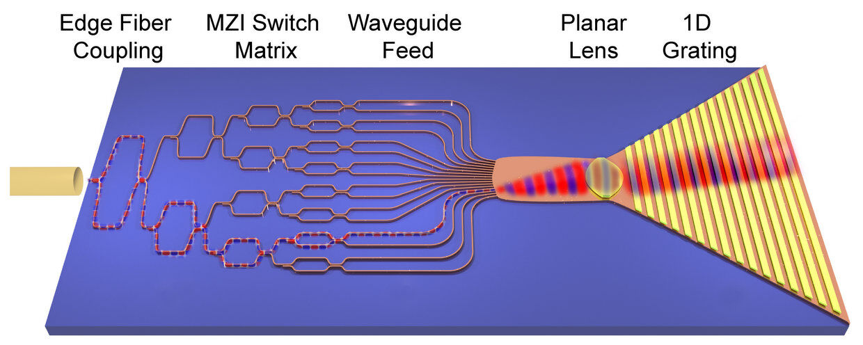
Solid-State LiDAR-on-a-chip system (courtesy of Dr. Scott Skirlo and IEEE).
Manufacturing, Packaging, and Testing — The Hidden Backbone of PIC Innovation
While the spotlight often shines on the performance of photonic integrated circuits, the real engineering challenge lies in manufacturing and packaging, the steps that determine yield, reliability, and scalability.
Wafer-Level Fabrication
The transition from lab prototypes to high-volume manufacturing relies on wafer-level photonics. Foundries such as AIM Photonics, IMEC, and Tower Semiconductor now offer MPW (Multi-Project Wafer) services, enabling researchers and startups to prototype PICs affordably. These platforms provide standardized building blocks, such as lasers, modulators, couplers, that can be customized through design kits, mirroring the approach that made CMOS electronics so successful.
Advanced Packaging and Fiber Coupling
Once fabricated, PICs must interface efficiently with the outside world. The alignment of optical fibers to submicron precision is a key challenge. New solutions like edge coupling, grating couplers, and photonic wire bonding are reducing assembly time and cost. Moreover, co-packaging optics (CPO) integrating photonics and electronics within a single package is emerging as the next frontier in optical interconnects. This architecture shortens electrical traces, reduces latency, and enables more compact switch systems for AI data centers.
Testing and Yield Optimization
Unlike electronic ICs, PICs require optical testing at every stage from wafer-level characterization to final packaging. Automated probe systems and integrated photodiodes are now being used for inline optical testing, drastically improving yield rates. Standardization efforts, such as those led by JEDEC and Photonics21, are helping define test metrics for insertion loss, crosstalk, and optical power, paving the way for scalable industrial adoption.
Integration Challenges and Future Directions
Despite the progress, several challenges remain before PICs become as ubiquitous as electronic ICs:
Coupling losses: Efficiently coupling light into and out of chips remains a precision challenge.
Thermal management: Heat affects wavelength stability in dense photonic circuits.
Laser integration: Silicon itself cannot emit light efficiently, requiring hybrid bonding of III–V materials.
Packaging complexity: Aligning optical fibers and ensuring reliability under thermal cycling adds cost and complexity.
Ongoing research is addressing these issues through:
Heterogeneous integration (III–V materials bonded onto silicon)
Wafer-level testing and automated optical alignment
3D photonic architectures and quantum-compatible PICs
Looking ahead, photonic integration will underpin not only communications and sensing but also quantum information processing, neuromorphic computing, and AI accelerators, where light offers unmatched parallelism and speed.
Conclusion
Photonic Integrated Circuits and Silicon Photonics mark a paradigm shift bringing the scalability of the semiconductor industry to the world of optics. From powering energy-efficient data centers to enabling compact biosensors and LIDAR systems, these technologies are at the heart of the next wave of photonic innovation. As integration challenges continue to be solved, the boundary between electronics and photonics will blur, giving rise to hybrid systems that define the future of computing, communication, and intelligent sensing.
References / Further Reading
IEEE Photonics Society – “Silicon Photonics for Data Centers” (2023)
Nature Photonics – “The Road to Integrated Photonics” (2022)
Intel White Paper – “Silicon Photonics: Scaling Optical Connectivity for the Data Era”
Optica Publishing – “Advances in Heterogeneous Integration for Photonic Chips” (2021)
MIT Lincoln Laboratory – “PICs for Sensing and Communication”
SPIE Proceedings – “Photonic Integration in LIDAR and Biomedical Systems”