
Scaling photonics from prototype to production and why it’s harder than in the field of electronics is the subject of this blog article.
This article is brought to you by Zolix Instruments, a leading manufacturer of motion control components and spectroscopy solutions.
Introduction: Scaling Photonics from Prototype to Production
In electronics, the journey from a working prototype to high-volume manufacturing is often predictable. Design rules are mature, fabrication processes are standardized, and supply chains are optimized for scale. In photonics, however, the story is very different. A device that performs beautifully in the lab can become unexpectedly complex, expensive, or even impractical when moved toward production.
This gap between prototype and production is one of the defining challenges of the photonics industry. It shapes not only how optical technologies are designed and manufactured, but also how they are evaluated, sourced, and brought to market. For many photonics companies, success is determined less by whether a concept works, and more by whether it can be produced reliably, repeatedly, and at a cost the market will accept.
Unlike electronics, where decades of scaling have smoothed the path from design to deployment, photonics often advances through application-specific solutions. Custom optics, specialized materials, tight tolerances, and manual processes remain common. These realities make scaling harder and they introduce uncertainty not just on the factory floor, but across the entire ecosystem that connects suppliers with buyers.
The same forces that make photonics difficult to scale – customization, tight tolerances, limited standardization, and fragile supply chains – also influence pricing, lead times, vendor selection, and buyer confidence. Understanding these constraints is essential for engineers and product teams, as well as for anyone navigating the photonics marketplace.
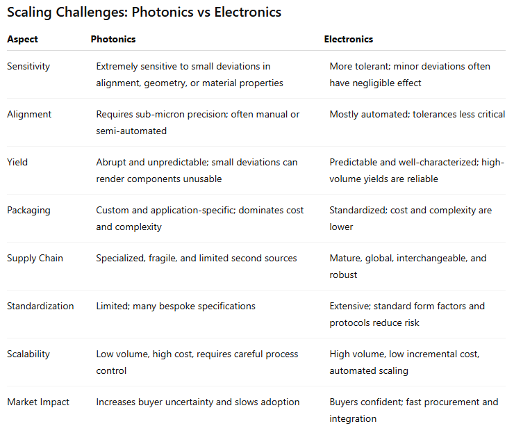
Why Scaling Works So Well in Electronics
Electronics benefits from decades of standardization and massive investment in manufacturing infrastructure. Transistors, interconnects, packaging, cables and testing methods follow well-established design rules. Once a circuit works, scaling it typically means reproducing the same process millions of times with high yield.
Key enablers include:
- Highly automated fabrication processes
- Mature electronic design automation (EDA) tools
- Tight process control at the nanometer scale
- Global, interchangeable supply chains
As a result, electronics manufacturing tolerates minor variations without significant performance penalties. Components are easily comparable across vendors, second sources are common, and production risks are well understood.
Scaling Photonics from Prototype to Production: Photonics Is Inherently Sensitive
Photonics systems interact directly with light, and light is unforgiving. Small deviations in alignment, surface quality, refractive index, or geometry can cause large performance changes. What works under controlled laboratory conditions may fail when exposed to manufacturing tolerances, temperature variations, or mechanical stress.
Unlike electrons in a conductor, photons are highly sensitive to:
- Surface roughness and contamination
- Angular misalignment on the order of microns
- Optical path length variations
- Polarization and mode structure
This sensitivity reduces tolerance for variability, making repeatability harder to achieve and increasing uncertainty as systems move toward production.
Alignment: The Silent Production Bottleneck
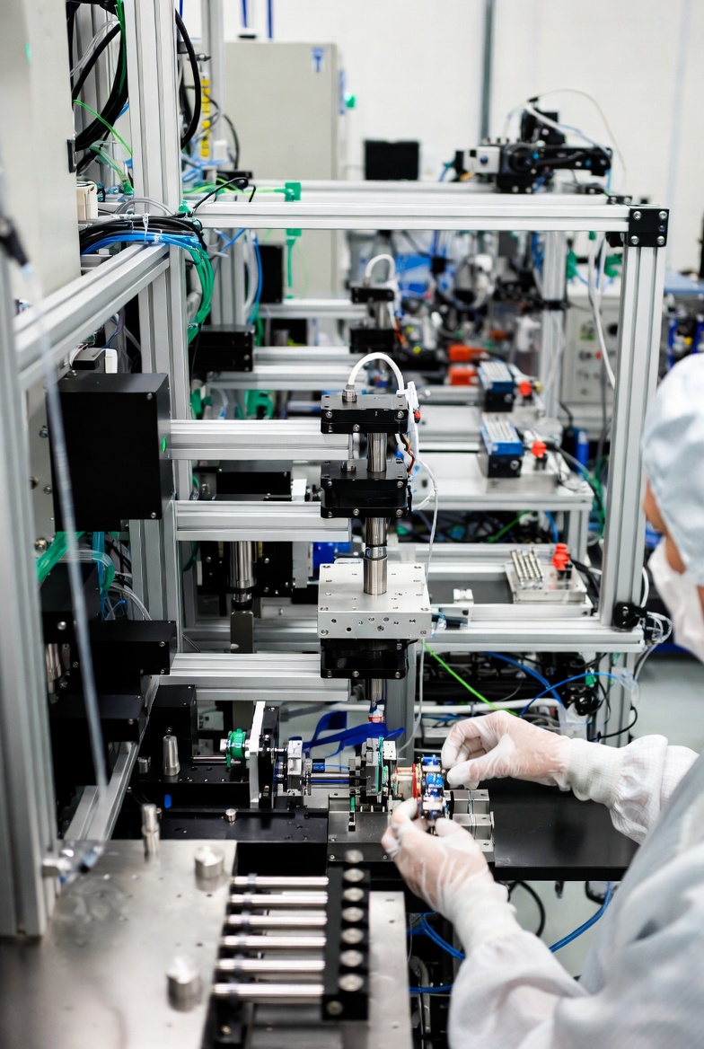
One of the most underestimated challenges in photonics manufacturing is alignment. Free-space optics, fiber coupling, and hybrid photonic assemblies often require sub-micron precision.
In a prototype environment, alignment is typically achieved manually by skilled engineers using active feedback. In production, manual alignment becomes slow, costly, and difficult to scale. Automating alignment adds capital expense and technical risk, especially when tolerances are tight and yields are uncertain.
Even in photonic integrated circuits, coupling light efficiently on and off chip remains a major hurdle. Packaging and alignment often dominate total system cost, far exceeding the cost of the photonic chip itself.
Yield Losses and Variability
Yield is a familiar concept in electronics manufacturing, but in photonics it behaves very differently. Yield losses tend to be sharper, less forgiving, and harder to predict. A deviation that would be electrically insignificant in an electronic circuit can be optically catastrophic, turning an otherwise functional component into scrap.
In photonics, performance often degrades nonlinearly. Small changes in geometry, material properties, or alignment can push a component outside its usable operating window. As a result, yield is not just a question of how many units pass inspection, but how tightly performance clusters around a target specification.
Common sources of yield loss include:
- Optical coating non-uniformity that alters reflectivity or transmission
- Waveguide sidewall roughness that increases scattering and loss
- Fiber attach or free-space coupling misalignment at the micron or sub-micron level
- Stress-induced birefringence from packaging or thermal mismatch
These effects are often cumulative. A component that is marginal in one dimension may fail entirely once combined with other tolerances during assembly.
Low production volumes compound the problem. Many photonics components are manufactured in batches that are too small to support robust statistical process control. Process drift can go unnoticed for long periods, and learning cycles are slower because feedback arrives infrequently.
For manufacturers, this variability increases cost, rework, and uncertainty during scale-up. For buyers, it complicates supplier qualification. Two components with identical datasheets may exhibit very different real-world performance, lot-to-lot consistency, or long-term stability. As a result, qualifying a photonics supplier often requires extensive testing, conservative margins, and long evaluation cycles.
This yield uncertainty reinforces cautious purchasing behavior across the photonics market and further slows the transition from prototype to production.
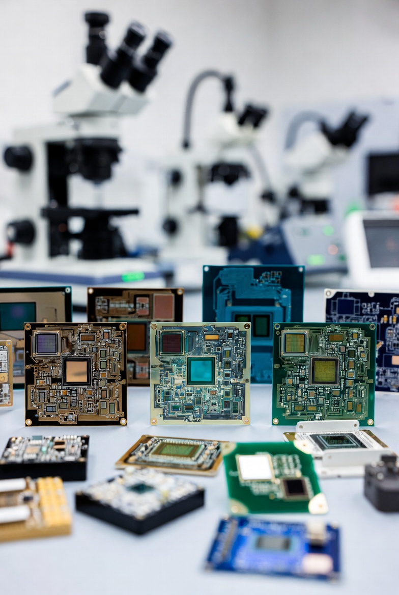
Packaging: Where Cost and Complexity Explode
Packaging is often described as the Achilles’ heel of photonics. While electronic packaging has converged around standardized form factors, photonics packaging remains fragmented and application-specific. Thermal management, optical access, mechanical stability, and environmental sealing must all be addressed simultaneously. In many cases, custom packages are developed for individual products, limiting reuse and economies of scale. This fragmentation drives up non-recurring engineering costs and slows time-to-market. It also makes it difficult for buyers to compare solutions or switch suppliers without significant redesign effort.
Supply Chain Fragility
Photonics supply chains are narrower and more specialized than their electronic counterparts. A single optical coating vendor, crystal grower, or fiber manufacturer can become a critical dependency.
Lead times are often long, minimum order quantities can be high, and second-source options may be limited or nonexistent. Scaling production under these conditions requires careful coordination and strong supplier relationships.
From a market perspective, this fragility reduces transparency. Components that appear similar on paper may differ significantly in manufacturability, availability, or long-term support, complicating sourcing decisions.
The Standardization Gap
Electronics thrives on standards: voltage levels, communication protocols, packaging footprints, and test methods. Photonics lacks comparable universal standards across many component categories.
While progress has been made in areas like telecom and datacom, many photonics applications still rely on custom specifications and bespoke interfaces. This increases integration effort and discourages modular design.
The absence of broad standardization affects not only engineering efficiency, but also how products are discovered, compared, and qualified in the marketplace.
When Photonic Integration Helps and When It Doesn’t
Photonic integrated circuits promise improved repeatability and reduced alignment complexity. In some applications, integration significantly improves scalability.
However, integration introduces its own challenges:
- Process variability across foundries
- Limited material platforms for certain wavelengths
- Trade-offs between performance and manufacturability
As a result, integration is not a universal solution. Many systems continue to rely on hybrid approaches that combine integrated and discrete components.
Bridging the Gap: Practical Strategies
Despite these challenges, there is significant progress with scaling in the photonics industry, and photonics products do reach volume production. Successful teams tend to adopt similar strategies:
- Designing for manufacturability early
- Accepting performance trade-offs to improve yield
- Reducing alignment degrees of freedom
- Working closely with manufacturing and packaging partners
These approaches favor robustness and repeatability over peak laboratory performance.
What This Means for Engineers and Product Teams
Understanding the realities of scaling photonics leads to better decisions early in the design process. Engineers who consider packaging, alignment, and supply chain constraints from the outset can avoid costly redesigns later.
For product teams, realistic expectations around cost, volume, lead times, and supplier availability are critical. Scaling photonics requires patience, cross-disciplinary collaboration, and an appreciation for trade-offs that extend beyond the lab.
Conclusion
Photonics enables technologies that electronics alone cannot deliver – from precision sensing to high-speed optical communication. Yet scaling photonics from prototype to production remains fundamentally harder than scaling electronics.
These challenges shape not only how photonics systems are built, but also how they are evaluated, sourced, and adopted. As manufacturing techniques mature and standardization improves, the gap will narrow. Until then, success in photonics depends on aligning engineering ambition with manufacturing reality and on navigating a marketplace shaped by the same constraints that govern light itself.