Successfully Advancing Next-Generation Optical Manufacturing and Semiconductor-Level Optical Integration
The global meta lens (metalens) market is expanding rapidly, with market size projected to reach the multi-billion-dollar level by 2031 and a compound annual growth rate (CAGR) approaching 80%. This growth is driven primarily by miniaturization and cost advantages enabled by semiconductor manufacturing processes, allowing meta lenses to penetrate a wide range of applications, including AR/VR, AI vision, 3D sensing, autonomous vehicles, and biomedical technologies. With its planar architecture and high efficiency, the meta lens is poised to accelerate the replacement of traditional optical lenses and become a standard component in next-generation optical chips.
LECC Technology has officially announced its latest mass-production meta lens laser module process technology. Leveraging wafer-level nanofabrication, the company has developed ultra-thin, fully planar optical components that overcome the limitations of conventional curved lenses, establishing a new benchmark for the miniaturization, integration, and performance of optical modules. Building on its proven track record in high-volume laser module manufacturing, already deployed in more than half of the world’s robotic vacuum cleaners, LECC brings production-scale reliability and yield control to next-generation meta lens integration.
The meta lens technology is manufactured using semiconductor-compatible processes on 12-inch wafers and has been validated for reflow and harsh operating environments, supporting operating temperature ranges from –40 °C to +125 °C. Multiple meta lens product families, including beam shapers, homogenizers, diffusers, and imaging meta lenses, are already in mass production, underscoring the technology’s readiness for commercial deployment.
The newly introduced technology employs nanoscale metasurface structures capable of precisely controlling the phase, amplitude, and polarization of light. High-precision manufacturing can be performed directly on 12-inch wafers, demonstrating LECC Technology’s strong expertise in laser modules, nanopatterning, and optical process technologies.
LECC Technology has also successfully integrated its meta lens process with a variety of optical materials, supporting multiple wavelength bands including visible light and near-infrared (NIR). Through wafer-level mass-production capability, meta lenses can be integrated into diverse laser modules, significantly enhancing optical performance, shortening optical path design, and reducing component thickness. These advantages contribute to improved system efficiency and yield, enabling applications across sensing, imaging, optical communications, and artificial intelligence devices.
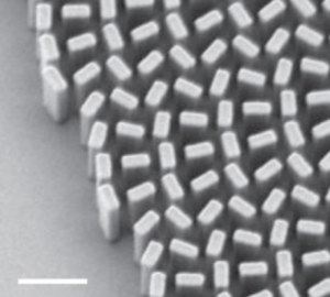
PB phase design. Schematic of metalens surface structures
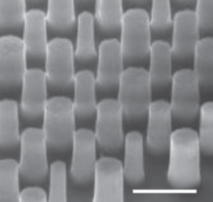
Propagation phase design
LECC Technology — Driving Industry-Wide Advancement with Nanometer-Scale Optical Processes
Mr. Hsin-Chih Tung, CEO of LECC Technology, stated:
“LECC Technology has long focused on the evolution of laser modules and continues to strengthen its technology roadmap for ultra-thin optical components through nanometer-scale process capabilities. We are pleased to successfully bring meta lens design and manufacturing into mass production for laser modules, enabling optical components to be integrated into wafer-level packaging using semiconductor processes. This overcomes the limitations of traditional optics in size, weight, and assembly. Looking ahead, meta lens technology will unlock new possibilities for wearable devices, smart terminals, automotive sensing, and precision measurement.”
Key Advantages of LECC Technology’s Meta Lens Process
One-Stop Integration from Design to Mass Production
- 12-Inch Wafer-Level Nanofabrication (Wafer-Level Meta Lens)
- High-Precision Nanostructure Processing (< 20 nm)
- Comprehensive Integrated Packaging (WLO / Optical Module Integration)
- Meta lenses can be integrated with image sensors, VCSELs, and ToF modules at the wafer level, reducing module thickness and improving optical coupling efficiency.
- High Yield and Large-Scale Mass Production Capability
Broad Industrial Applications of Meta Lens Technology
From Consumer Electronics to AI and Defense
LECC Technology’s meta lens solutions can be widely applied to:
- 3D depth sensing, ToF, and structured light systems
- LiDAR, spatial sensing, defense, and aerospace technologies
- Physiological signal sensing and AI-enabled sensors
- Biomedical miniature imaging and endoscopic probes
- Smartphone optical modules (NIR / SWIR)
- AR/VR near-eye displays and eye-tracking systems
- Optical communications and silicon photonics components
By enabling optical modules that are lighter, thinner, and easier to integrate, meta lens technology accelerates product miniaturization and high-performance system development.
Commercial Availability and Product Scope
LECC Technology’s meta lens portfolio already includes multiple production-ready product families, covering beam shaping and imaging applications. These include line diffusers, homogenizers, random and multi-spot beam shapers, collimators, and imaging meta lenses designed for use with VCSELs and image sensors. Several models supporting common wavelengths such as 850 nm and 940 nm are already in volume production, while additional configurations are under active development. This breadth of available products demonstrates LECC Technology’s ability to translate meta lens designs into commercially manufacturable, application-ready optical components.
Embracing the Next Generation of Optical Components
LECC Technology emphasizes that as AI, robotics, wearable devices, and silicon photonics continue to advance, wafer-level optical integration will become the mainstream approach, with meta lenses emerging as one of the most critical enabling components. Leveraging its nanometer-scale process capabilities, stable mass-production platforms, and cross-disciplinary collaboration model, LECC Technology aims to accelerate the adoption of meta lens technology across consumer electronics, industrial, medical, and defense markets.
About LECC Technology
More than one out of every two robotic vacuum cleaners worldwide uses LECC laser modules. In the medical field, computed tomography (CT) scanners from leading manufacturers such as Siemens, GE, and Philips also incorporate LECC laser modules. LECC products are exported to Europe, the Americas, Japan, China, and other global markets, establishing the company as a true “hidden champion” in the photonics and laser industry.