Inverse design in photonics fueled by AI is the topic of this blog article.
Courtesy of Professor Vuckovic’s research group at Stanford
This article is brought to you by the support of Zolix Instruments, a leading manufacturer of motion control and spectroscopy solutions.
Introduction – From Intuition to Optimization
For decades, designing optical components has relied on human intuition and analytical modeling. Engineers began with a geometry of a lens curvature, grating spacing, or cavity structure and adjusted parameters until the device met performance goals. While effective for simple optics, this approach struggles with the complexity of modern photonics, where nanostructures, metasurfaces, and integrated devices require precise control of light on sub-wavelength scales.
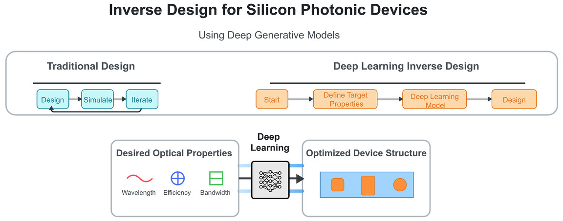
Enter inverse design in photonics, a paradigm shift where engineers define what they want light to do, and algorithms determine how to achieve it. Enabled by artificial intelligence (AI), machine learning, and advanced optimization techniques, inverse design has become one of the most transformative tools in optical engineering today.
What Is Inverse Design in Photonics?
In traditional (“forward”) design, you start with a structure and calculate its optical behavior using Maxwell’s equations or numerical solvers like FDTD (Finite-Difference Time-Domain). In inverse design, the process is reversed: you specify the desired optical response, such as maximizing light transmission, achieving a specific phase shift, or splitting wavelengths, and let algorithms iteratively modify the structure until that target is achieved.
This concept is similar to topology optimization in mechanical engineering, but applied to the electromagnetic domain. The algorithm explores millions of possible geometries, guided by gradients or AI models, to find unconventional yet high-performing optical designs that would be difficult or impossible to conceive manually.
Example of an inverse design workflow (courtesy of Sun Jae Baek and Minhyeok Lee )
How It Works – From Physics to Algorithms
Inverse design involves a few key computational steps:
Define the performance goal: For example, maximize coupling efficiency between a fiber and a silicon waveguide.
Choose a design region: A 2D or 3D space where material distribution can vary (e.g., silicon vs. air).
Simulate light propagation: Using electromagnetic solvers (FDTD, FEM, RCWA).
Compute gradients: The adjoint method efficiently determines how small geometry changes affect performance.
Iterate and optimize: Algorithms like gradient descent, genetic algorithms, or deep learning adjust the design until convergence.
AI and neural networks accelerate this process by predicting optical responses without solving Maxwell’s equations every iteration. This drastically reduces computation time, making large-scale design feasible.
Algorithms Behind Inverse Design
There are several algorithmic approaches driving progress in this field:
Adjoint Method: Calculates gradients with respect to every design parameter in a single simulation, enabling optimization of thousands of variables efficiently.
Topology Optimization: Continuously varies material density in each voxel or pixel to find optimal material layouts.
Evolutionary and Genetic Algorithms: Explore global design space using “survival of the fittest” principles to avoid local minima.
Deep Learning and Surrogate Models: AI models learn from prior simulations to predict outcomes and guide optimization faster than brute-force physics solvers.
In cutting-edge research, hybrid methods combine physics-based modeling with machine learning, balancing accuracy and speed. For instance, neural networks are trained to approximate electromagnetic fields, then refined with physics-constrained feedback loops.
Applications of Inverse Design in Photonics
Inverse design has already produced remarkable breakthroughs across multiple photonics subfields:
Metasurfaces and Flat Optics
AI-optimized metasurfaces achieve precise control over light’s amplitude, phase, and polarization enabling ultra-thin lenses, beam deflectors, and holographic displays. Designs generated by inverse optimization outperform hand-engineered versions in focusing efficiency and bandwidth.
On-Chip Photonics
In silicon photonics, inverse-designed components such as wavelength demultiplexers, mode converters, and couplers occupy a fraction of the footprint of traditional designs while maintaining or even improving performance.
Laser and Resonator Engineering
Inverse design has produced high-Q microresonators, custom laser cavities, and low-loss grating couplers, accelerating advances in integrated laser systems and optical communications.
AR/VR and Imaging Optics
Compact freeform optics optimized through AI-based inverse design are being integrated into AR/VR headsets, enabling lightweight systems with wide fields of view and minimal aberrations.
Quantum and Nonlinear Photonics
Designing waveguides and cavities for quantum light sources, entangled photon pairs, and nonlinear frequency conversion benefits greatly from the precision of inverse design, pushing the limits of efficiency and coherence.
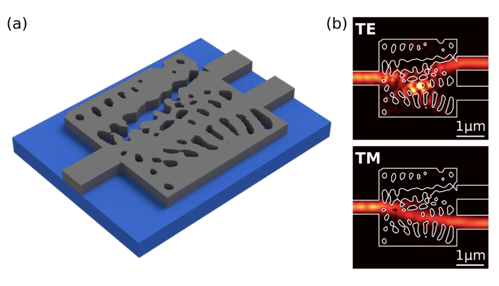
Case Study – Inverse-Designed Wavelength Splitter
A notable demonstration comes from Stanford University’s research group led by Jelena Vučković. Using inverse design, the team created a wavelength demultiplexer just a few microns long that separates 1300 nm and 1550 nm light on a silicon chip. Traditional designs would require hundreds of microns. The optimized device achieved >90% efficiency and <1 dB insertion loss, validating the power of algorithmic design in integrated photonics.
Benefits of Inverse Design
Ultra-Compact Devices: Achieves miniaturization beyond what traditional parametric design allows.
High Performance: Optimized for multiple objectives (e.g., efficiency, bandwidth, polarization control).
Novel Functionalities: Produces geometries not intuitive to human designers.
Automation: Reduces manual iteration time and human bias.
Design Portability: Works across wavelength regimes — from visible to terahertz.
Challenges and Limitations
While promising, inverse design faces technical and practical challenges:
Fabrication Constraints: Some optimized shapes are difficult to manufacture using current lithographic or etching techniques.
Computation Costs: Full 3D electromagnetic optimization remains computationally expensive.
Interpretability: Designs can be “black boxes”, effective, but hard to understand physically.
Generalization: AI-trained models may fail outside their training data, requiring hybrid verification with physics simulations.
Research continues to focus on physics-informed neural networks (PINNs) and fabrication-aware optimization to address these issues.
Future Outlook — AI-Driven Photonics Design Automation
As AI models mature, inverse design is evolving toward fully automated photonics design pipelines, integrating simulation, fabrication constraints, and experimental validation. Future systems could autonomously generate ready-to-fabricate device blueprints based on desired optical functionality.
Moreover, coupling quantum computing with inverse photonic design could unlock unprecedented capabilities in optimizing ultra-complex optical systems for telecommunications, sensing, and quantum information processing.
The convergence of AI, computational physics, and photonic fabrication will likely define the next decade of innovation leading toward a new era of self-designed optics.
Conclusion
Inverse design represents a paradigm shift from traditional trial-and-error methods to goal-oriented, data-driven photonics engineering. By merging AI algorithms with electromagnetic theory, engineers are unlocking optical functionalities that were once unimaginable from submicron couplers to ultrathin metasurfaces and high-Q resonators.
As computational resources expand and fabrication catches up, AI-optimized photonic design will not only accelerate research but also democratize innovation enabling faster prototyping, lower costs, and smarter optical systems across industries.
References
Molesky, S., Lin, Z., Piggott, A. Y., Jin, W., Vučković, J., & Rodriguez, A. W. (2018). Inverse design in nanophotonics. Nature Photonics, 12(11), 659–670.
Piggott, A. Y., et al. (2015). Inverse design and demonstration of a compact and broadband on-chip wavelength demultiplexer. Nature Photonics, 9(6), 374–377.
Jensen, J. S., & Sigmund, O. (2011). Topology optimization for nano-photonics. Laser & Photonics Reviews, 5(2), 308–321.
Ma, W., Cheng, F., & Liu, Y. (2021). Deep-learning-enabled on-demand design of photonic devices. Nature Photonics, 15(1), 77–90.
Sell, D., Yang, J., Doshay, S., & Fan, J. A. (2017). Large-angle, multifunctional metagratings based on freeform multimode geometries. Nano Letters, 17(6), 3752–3757.